正在加载图片...
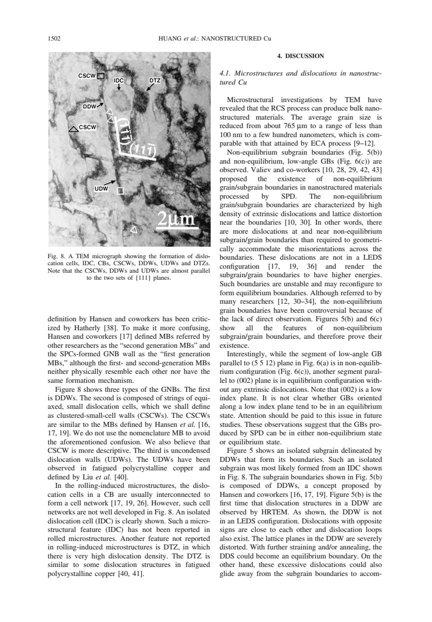
1502 HUANG et al:NANOSTRUCTURED Cu 4.DISCUSSION cscw 4.1.Microstructures and dislocations in nanostruc- tured Cu Microstructural investigations by TEM have DDW revealed that the RCS process can produce bulk nano- structured materials.The average grain size is CSCW reduced from about 765 um to a range of less than 100 nm to a few hundred nanometers,which is com- parable with that attained by ECA process [9-12]. Non-equilibrium subgrain boundaries (Fig.5(b)) and non-equilibrium,low-angle GBs (Fig.6(c))are observed.Valiev and co-workers [10,28,29,42,43] proposed the existence of non-equilibrium UDW grain/subgrain boundaries in nanostructured materials processed by SPD.The non-equilibrium grain/subgrain boundaries are characterized by high density of extrinsic dislocations and lattice distortion near the boundaries [10,30].In other words,there are more dislocations at and near non-equilibrium subgrain/grain boundaries than required to geometri- cally accommodate the misorientations across the Fig.8.A TEM micrograph showing the formation of dislo- boundaries.These dislocations are not in a LEDS cation cells,IDC,CBs,CSCWs,DDWs,UDWs and DTZs Note that the CSCWs,DDWs and UDWs are almost parallel configuration [17,19,36]and render the to the two sets of (111)planes. subgrain/grain boundaries to have higher energies. Such boundaries are unstable and may reconfigure to form equilibrium boundaries.Although referred to by many researchers [12,30-34],the non-equilibrium grain boundaries have been controversial because of definition by Hansen and coworkers has been critic- the lack of direct observation.Figures 5(b)and 6(c) ized by Hatherly [38].To make it more confusing, show all the features of non-equilibrium Hansen and coworkers [17]defined MBs referred by subgrain/grain boundaries,and therefore prove their other researchers as the "second generation MBs"and existence the SPCs-formed GNB wall as the "first generation Interestingly,while the segment of low-angle GB MBs."although the first-and second-generation MBs parallel to (55 12)plane in Fig.6(a)is in non-equilib- neither physically resemble each other nor have the rium configuration(Fig.6(c)),another segment paral- same formation mechanism. lel to (002)plane is in equilibrium configuration with- Figure 8 shows three types of the GNBs.The first out any extrinsic dislocations.Note that(002)is a low is DDWs.The second is composed of strings of equi- index plane.It is not clear whether GBs oriented axed,small dislocation cells,which we shall define along a low index plane tend to be in an equilibrium as clustered-small-cell walls(CSCWs).The CSCWs state.Attention should be paid to this issue in future are similar to the MBs defined by Hansen et al.[16, studies.These observations suggest that the GBs pro- 17.191.We do not use the nomenclature MB to avoid duced by SPD can be in either non-equilibrium state the aforementioned confusion.We also believe that or equilibrium state. CSCW is more descriptive.The third is uncondensed Figure 5 shows an isolated subgrain delineated by dislocation walls (UDWs).The UDWs have been DDWs that form its boundaries.Such an isolated observed in fatigued polycrystalline copper and subgrain was most likely formed from an IDC shown defined by Liu et al.[40]. in Fig.8.The subgrain boundaries shown in Fig.5(b) In the rolling-induced microstructures,the dislo- is composed of DDWs,a concept proposed by cation cells in a CB are usually interconnected to Hansen and coworkers [16,17,19].Figure 5(b)is the form a cell network [17,19,261.However,such cell first time that dislocation structures in a DDW are networks are not well developed in Fig.8.An isolated observed by HRTEM.As shown,the DDW is not dislocation cell (IDC)is clearly shown.Such a micro- in an LEDS configuration.Dislocations with opposite structural feature (IDC)has not been reported in signs are close to each other and dislocation loops rolled microstructures.Another feature not reported also exist.The lattice planes in the DDW are severely in rolling-induced microstructures is DTZ,in which distorted.With further straining and/or annealing.the there is very high dislocation density.The DTZ is DDS could become an equilibrium boundary.On the similar to some dislocation structures in fatigued other hand,these excessive dislocations could also polycrystalline copper [40,41]. glide away from the subgrain boundaries to accom-1502 HUANG et al.: NANOSTRUCTURED Cu Fig. 8. A TEM micrograph showing the formation of dislocation cells, IDC, CBs, CSCWs, DDWs, UDWs and DTZs. Note that the CSCWs, DDWs and UDWs are almost parallel to the two sets of {111} planes. definition by Hansen and coworkers has been criticized by Hatherly [38]. To make it more confusing, Hansen and coworkers [17] defined MBs referred by other researchers as the “second generation MBs” and the SPCs-formed GNB wall as the “first generation MBs,” although the first- and second-generation MBs neither physically resemble each other nor have the same formation mechanism. Figure 8 shows three types of the GNBs. The first is DDWs. The second is composed of strings of equiaxed, small dislocation cells, which we shall define as clustered-small-cell walls (CSCWs). The CSCWs are similar to the MBs defined by Hansen et al. [16, 17, 19]. We do not use the nomenclature MB to avoid the aforementioned confusion. We also believe that CSCW is more descriptive. The third is uncondensed dislocation walls (UDWs). The UDWs have been observed in fatigued polycrystalline copper and defined by Liu et al. [40]. In the rolling-induced microstructures, the dislocation cells in a CB are usually interconnected to form a cell network [17, 19, 26]. However, such cell networks are not well developed in Fig. 8. An isolated dislocation cell (IDC) is clearly shown. Such a microstructural feature (IDC) has not been reported in rolled microstructures. Another feature not reported in rolling-induced microstructures is DTZ, in which there is very high dislocation density. The DTZ is similar to some dislocation structures in fatigued polycrystalline copper [40, 41]. 4. DISCUSSION 4.1. Microstructures and dislocations in nanostructured Cu Microstructural investigations by TEM have revealed that the RCS process can produce bulk nanostructured materials. The average grain size is reduced from about 765 µm to a range of less than 100 nm to a few hundred nanometers, which is comparable with that attained by ECA process [9–12]. Non-equilibrium subgrain boundaries (Fig. 5(b)) and non-equilibrium, low-angle GBs (Fig. 6(c)) are observed. Valiev and co-workers [10, 28, 29, 42, 43] proposed the existence of non-equilibrium grain/subgrain boundaries in nanostructured materials processed by SPD. The non-equilibrium grain/subgrain boundaries are characterized by high density of extrinsic dislocations and lattice distortion near the boundaries [10, 30]. In other words, there are more dislocations at and near non-equilibrium subgrain/grain boundaries than required to geometrically accommodate the misorientations across the boundaries. These dislocations are not in a LEDS configuration [17, 19, 36] and render the subgrain/grain boundaries to have higher energies. Such boundaries are unstable and may reconfigure to form equilibrium boundaries. Although referred to by many researchers [12, 30–34], the non-equilibrium grain boundaries have been controversial because of the lack of direct observation. Figures 5(b) and 6(c) show all the features of non-equilibrium subgrain/grain boundaries, and therefore prove their existence. Interestingly, while the segment of low-angle GB parallel to (5 5 12) plane in Fig. 6(a) is in non-equilibrium configuration (Fig. 6(c)), another segment parallel to (002) plane is in equilibrium configuration without any extrinsic dislocations. Note that (002) is a low index plane. It is not clear whether GBs oriented along a low index plane tend to be in an equilibrium state. Attention should be paid to this issue in future studies. These observations suggest that the GBs produced by SPD can be in either non-equilibrium state or equilibrium state. Figure 5 shows an isolated subgrain delineated by DDWs that form its boundaries. Such an isolated subgrain was most likely formed from an IDC shown in Fig. 8. The subgrain boundaries shown in Fig. 5(b) is composed of DDWs, a concept proposed by Hansen and coworkers [16, 17, 19]. Figure 5(b) is the first time that dislocation structures in a DDW are observed by HRTEM. As shown, the DDW is not in an LEDS configuration. Dislocations with opposite signs are close to each other and dislocation loops also exist. The lattice planes in the DDW are severely distorted. With further straining and/or annealing, the DDS could become an equilibrium boundary. On the other hand, these excessive dislocations could also glide away from the subgrain boundaries to accom-