正在加载图片...
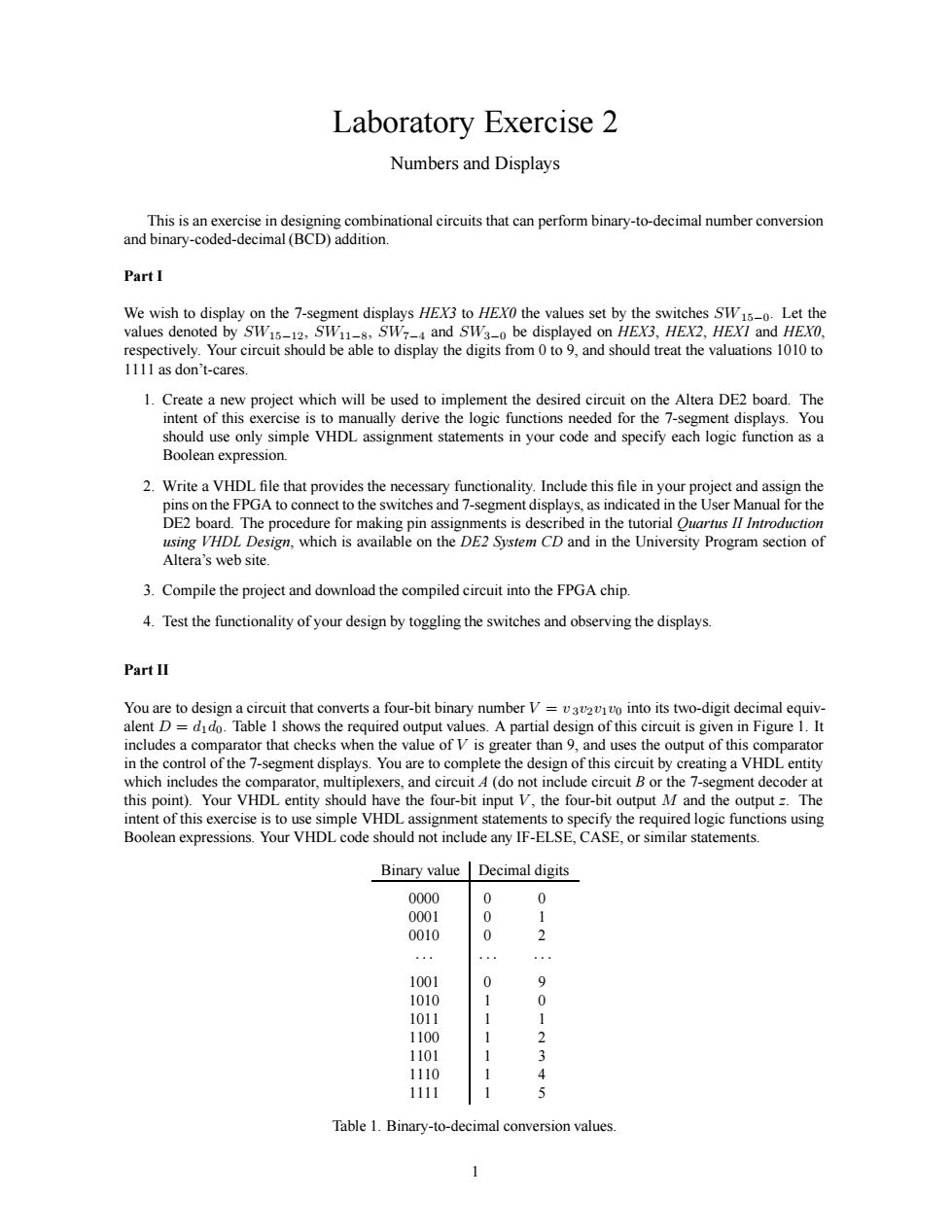
Laboratory Exercise 2 Numbers and Displays This is an exercise in designing combinational circuits that can perform binary-to-decimal number conversion and binary-coded-decimal(BCD)addition. PartI We wish to display on the 7-segment displays HEX3 to HEXO the values set by the switches SW 1 Create a roiect which will be ent the desired ci cuit on the altera de2 board The y simple VHDL assignment statements in your code and specify each logic function as a clude this ile DE2 poard The procedure for makinnassimnts is deseribed in the tutoral on theDnd theoof 3.Compile the project and download the compiled circuit into the FPGA chip. 4.Test the functionality of your design by toggling the switches and observing the displays PartII 一”网b 1 hat in thecorotsegment displays.You are tocompetthe design of thiscrt byreating VHDLnit nludes the comparaor muplexers.and circuit 4(do not include circuit B or the seg egment decoder a entity sho e the fou-bit input v. the four-bit output M an e0up2. .Your shoul not include any IF-ELSE,CASE.r smar statemens Binary value Decimal digits 0000 0 100 0 9 0 1101 1111 3 Table 1.Binary-to-decimal conversion values.Laboratory Exercise 2 Numbers and Displays This is an exercise in designing combinational circuits that can perform binary-to-decimal number conversion and binary-coded-decimal (BCD) addition. Part I We wish to display on the 7-segment displays HEX3 to HEX0 the values set by the switches SW15−0. Let the values denoted by SW15−12, SW11−8, SW7−4 and SW3−0 be displayed on HEX3, HEX2, HEX1 and HEX0, respectively. Your circuit should be able to display the digits from 0 to 9, and should treat the valuations 1010 to 1111 as don’t-cares. 1. Create a new project which will be used to implement the desired circuit on the Altera DE2 board. The intent of this exercise is to manually derive the logic functions needed for the 7-segment displays. You should use only simple VHDL assignment statements in your code and specify each logic function as a Boolean expression. 2. Write a VHDL file that provides the necessary functionality. Include this file in your project and assign the pins on the FPGA to connect to the switches and 7-segment displays, as indicated in the User Manual for the DE2 board. The procedure for making pin assignments is described in the tutorial Quartus II Introduction using VHDL Design, which is available on the DE2 System CD and in the University Program section of Altera’s web site. 3. Compile the project and download the compiled circuit into the FPGA chip. 4. Test the functionality of your design by toggling the switches and observing the displays. Part II You are to design a circuit that converts a four-bit binary number V = v 3v2v1v0 into its two-digit decimal equivalent D = d1d0. Table 1 shows the required output values. A partial design of this circuit is given in Figure 1. It includes a comparator that checks when the value of V is greater than 9, and uses the output of this comparator in the control of the 7-segment displays. You are to complete the design of this circuit by creating a VHDL entity which includes the comparator, multiplexers, and circuit A (do not include circuit B or the 7-segment decoder at this point). Your VHDL entity should have the four-bit input V , the four-bit output M and the output z. The intent of this exercise is to use simple VHDL assignment statements to specify the required logic functions using Boolean expressions. Your VHDL code should not include any IF-ELSE, CASE, or similar statements. Binary value Decimal digits 0000 0 0 0001 0 1 0010 0 2 ... ... ... 1001 0 9 1010 1 0 1011 1 1 1100 1 2 1101 1 3 1110 1 4 1111 1 5 Table 1. Binary-to-decimal conversion values. 1