正在加载图片...
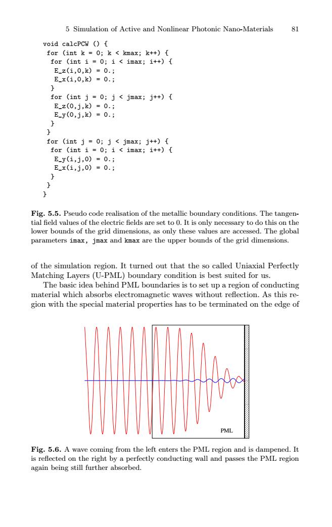
5 Simulation of Active and Nonlinear Photonic Nano-Materials 81 void calcPCW () for (int k 0;k kmax;k++){ for (int i=0;i<imax;i++){ Ez(1,0,k)=0.; Ex(1,0,k)=0.; 2 for (int j=0;j<jmax;j++){ E_z(0,j,k)=0.; E_-y(0,j,)=0.; d 2 for (int j=0;j<jmax;j++){ for (int i=0;i<imax;i++){ E_-y(i,j,0)=0.; E_x(1,j,0)=0.; } Fig.5.5.Pseudo code realisation of the metallic boundary conditions.The tangen- tial field values of the electric fields are set to 0.It is only necessary to do this on the lower bounds of the grid dimensions,as only these values are accessed.The global parameters imax,jmax and kmax are the upper bounds of the grid dimensions. of the simulation region.It turned out that the so called Uniaxial Perfectly Matching Layers(U-PML)boundary condition is best suited for us. The basic idea behind PML boundaries is to set up a region of conducting material which absorbs electromagnetic waves without reflection.As this re- gion with the special material properties has to be terminated on the edge of PML Fig.5.6.A wave coming from the left enters the PML region and is dampened.It is reflected on the right by a perfectly conducting wall and passes the PML region again being still further absorbed.5 Simulation of Active and Nonlinear Photonic Nano-Materials 81 void calcPCW () { for (int k = 0; k < kmax; k++) { for (int i = 0; i < imax; i++) { E_z(i,0,k) = 0.; E_x(i,0,k) = 0.; } for (int j = 0; j < jmax; j++) { E_z(0,j,k) = 0.; E_y(0,j,k) = 0.; } } for (int j = 0; j < jmax; j++) { for (int i = 0; i < imax; i++) { E_y(i,j,0) = 0.; E_x(i,j,0) = 0.; } } } Fig. 5.5. Pseudo code realisation of the metallic boundary conditions. The tangential field values of the electric fields are set to 0. It is only necessary to do this on the lower bounds of the grid dimensions, as only these values are accessed. The global parameters imax, jmax and kmax are the upper bounds of the grid dimensions. of the simulation region. It turned out that the so called Uniaxial Perfectly Matching Layers (U-PML) boundary condition is best suited for us. The basic idea behind PML boundaries is to set up a region of conducting material which absorbs electromagnetic waves without reflection. As this region with the special material properties has to be terminated on the edge of PML Fig. 5.6. A wave coming from the left enters the PML region and is dampened. It is reflected on the right by a perfectly conducting wall and passes the PML region again being still further absorbed