正在加载图片...
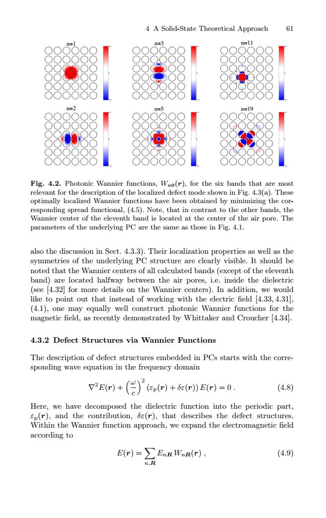
4 A Solid-State Theoretical Approach 61 19 Fig.4.2.Photonic Wannier functions,Wno(r),for the six bands that are most relevant for the description of the localized defect mode shown in Fig.4.3(a).These optimally localized Wannier functions have been obtained by minimizing the cor- responding spread functional,(4.5).Note,that in contrast to the other bands,the Wannier center of the eleventh band is located at the center of the air pore.The parameters of the underlying PC are the same as those in Fig.4.1. also the discussion in Sect.4.3.3).Their localization properties as well as the symmetries of the underlying PC structure are clearly visible.It should be noted that the Wannier centers of all calculated bands (except of the eleventh band)are located halfway between the air pores,i.e.inside the dielectric (see [4.32]for more details on the Wannier centers).In addition,we would like to point out that instead of working with the electric field [4.33,4.31, (4.1),one may equally well construct photonic Wannier functions for the magnetic field,as recently demonstrated by Whittaker and Croucher [4.34. 4.3.2 Defect Structures via Wannier Functions The description of defect structures embedded in PCs starts with the corre- sponding wave equation in the frequency domain 2 V2E(r) ( (Ep(r)+6s(r))E(r)=0. (4.8) Here,we have decomposed the dielectric function into the periodic part, Ep(r),and the contribution,s(r),that describes the defect structures. Within the Wannier function approach,we expand the electromagnetic field according to E(r)=∑EnRWnR(r), (4.9) n.R4 A Solid-State Theoretical Approach 61 n=1 n=2 n=3 n=5 n=11 n=19 Fig. 4.2. Photonic Wannier functions, Wn0(r), for the six bands that are most relevant for the description of the localized defect mode shown in Fig. 4.3(a). These optimally localized Wannier functions have been obtained by minimizing the corresponding spread functional, (4.5). Note, that in contrast to the other bands, the Wannier center of the eleventh band is located at the center of the air pore. The parameters of the underlying PC are the same as those in Fig. 4.1. also the discussion in Sect. 4.3.3). Their localization properties as well as the symmetries of the underlying PC structure are clearly visible. It should be noted that the Wannier centers of all calculated bands (except of the eleventh band) are located halfway between the air pores, i.e. inside the dielectric (see [4.32] for more details on the Wannier centers). In addition, we would like to point out that instead of working with the electric field [4.33, 4.31], (4.1), one may equally well construct photonic Wannier functions for the magnetic field, as recently demonstrated by Whittaker and Croucher [4.34]. 4.3.2 Defect Structures via Wannier Functions The description of defect structures embedded in PCs starts with the corresponding wave equation in the frequency domain ∇2E(r) + ω c 2 (εp(r) + δε(r)) E(r)=0 . (4.8) Here, we have decomposed the dielectric function into the periodic part, εp(r), and the contribution, δε(r), that describes the defect structures. Within the Wannier function approach, we expand the electromagnetic field according to E(r) = n,R EnR WnR(r) , (4.9)