正在加载图片...
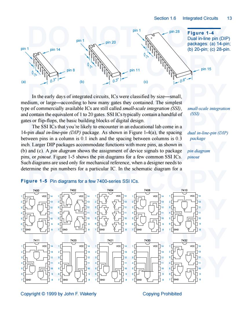
Section1.6 Integrated Circuits 13 Figure 1-4 Dual in-line pin (DIP) pin 20 packages:(a)14-pin; pin 14 (b)20-pin;(c)28-pin. 011 pin 15 a.6 In the early days of integrated circuits,ICs were classified by size-small. medium,or large small-scale integration and contain the equivalent of I to 20 gates.SSI ICs typically contain a handful of (SSI) gates or flip-flops,the basic building blocks of digital design. The SSI ICs that you're likely to encounter in an educational lab come in a 14-pin dual in-line-pin (DIP)package.As shown in Figure 1-4(a),the spacing dual in-line-pin (DIP) between pins in a column is 0.1 inch and the spacing between columns is 0.3 package inch.Larger DIP packages accommodate functions with more pins,as shown in (b)and(c).A pin diagram shows the assignment of device signals to package pin diagram pins,or pinout.Figure 1-5 shows the pin diagrams for a few common SSI ICs. pinout Such diagrams are used only for mechanical reference,when a designer needs to determine the pin numbers for a particular IC.In the schematic diagram for a Figure 1-5 Pin diagrams for a few 7400-series SSI ICs 四在网 Copyright 1999 by John F.Wakerly Copying ProhibitedSection 1.6 Integrated Circuits 13 DO NOT COPY DO NOT COPY DO NOT COPY DO NOT COPY DO NOT COPY DO NOT COPY DO NOT COPY DO NOT COPY DO NOT COPY Copyright © 1999 by John F. Wakerly Copying Prohibited In the early days of integrated circuits, ICs were classified by size—small, medium, or large—according to how many gates they contained. The simplest type of commercially available ICs are still called small-scale integration (SSI), and contain the equivalent of 1 to 20 gates. SSI ICs typically contain a handful of gates or flip-flops, the basic building blocks of digital design. The SSI ICs that you’re likely to encounter in an educational lab come in a 14-pin dual in-line-pin (DIP) package. As shown in Figure 1-4(a), the spacing between pins in a column is 0.1 inch and the spacing between columns is 0.3 inch. Larger DIP packages accommodate functions with more pins, as shown in (b) and (c). A pin diagram shows the assignment of device signals to package pins, or pinout. Figure 1-5 shows the pin diagrams for a few common SSI ICs. Such diagrams are used only for mechanical reference, when a designer needs to determine the pin numbers for a particular IC. In the schematic diagram for a small-scale integration (SSI) dual in-line-pin (DIP) package (a) 0.3" (b) (c) 0.1" pin 1 pin 14 pin 8 0.1" pin 1 pin 20 0.3" pin 11 0.6" 0.1" pin 1 pin 28 pin 15 Figure 1-4 Dual in-line pin (DIP) packages: (a) 14-pin; (b) 20-pin; (c) 28-pin. pin diagram pinout 1 2 3 4 5 6 7 14 13 12 11 10 9 GND 8 VCC 7400 1 2 3 4 5 6 7 14 13 12 11 10 9 GND 8 VCC 7402 1 2 3 4 5 6 7 14 13 12 11 10 9 GND 8 VCC 7404 1 2 3 4 5 6 7 14 13 12 11 10 9 GND 8 VCC 7410 1 2 3 4 5 6 7 14 13 12 11 10 9 GND 8 VCC 7411 1 2 3 4 5 6 7 14 13 12 11 10 9 GND 8 VCC 7420 1 2 3 4 5 6 7 14 13 12 11 10 9 GND 8 VCC 7421 1 2 3 4 5 6 7 14 13 12 11 10 9 GND 8 VCC 7430 1 2 3 4 5 6 7 14 13 12 11 10 9 GND 8 VCC 7432 1 2 3 4 5 6 7 14 13 12 11 10 9 GND 8 VCC 7408 Figure 1-5 Pin diagrams for a few 7400-series SSI ICs