正在加载图片...

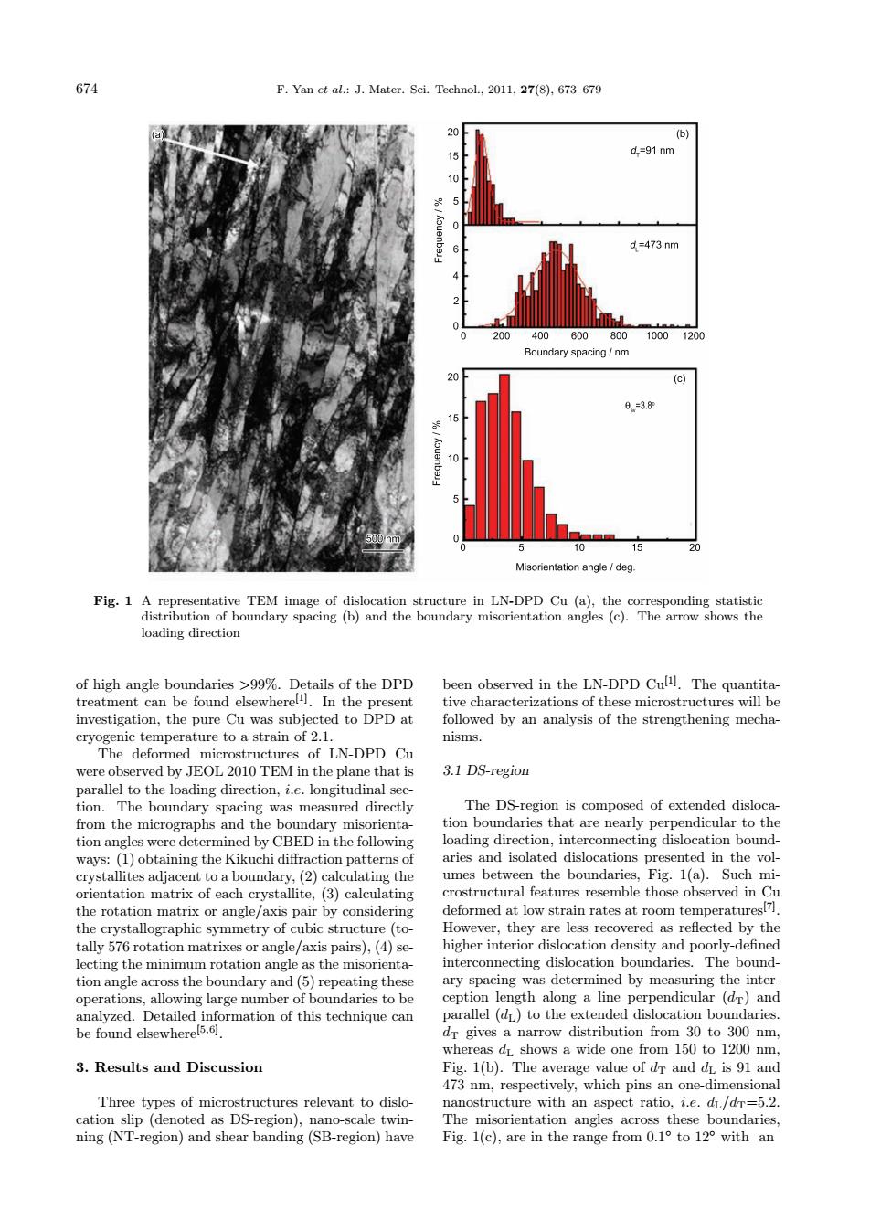
674 F.Yan et al.:J.Mater.Sci.Technol.,2011,27(8),673-679 20 161 15 d=91 nm 10 d =473 nm h 200 400 600 800 10001200 Boundary spacing /nm 20 8=3.8° 40 5 10 15 Misorientation angle deg. Fig.1 A representative TEM image of dislocation structure in LN-DPD Cu (a),the corresponding statistic distribution of boundary spacing (b)and the boundary misorientation angles (c).The arrow shows the loading direction of high angle boundaries >99%.Details of the DPD been observed in the LN-DPD Culll.The quantita- treatment can be found elsewherell.In the present tive characterizations of these microstructures will be investigation,the pure Cu was subjected to DPD at followed by an analysis of the strengthening mecha- cryogenic temperature to a strain of 2.1. nisms. The deformed microstructures of LN-DPD Cu were observed by JEOL 2010 TEM in the plane that is 3.1 DS-region parallel to the loading direction,i.e.longitudinal sec- tion.The boundary spacing was measured directly The DS-region is composed of extended disloca- from the micrographs and the boundary misorienta- tion boundaries that are nearly perpendicular to the tion angles were determined by CBED in the following loading direction,interconnecting dislocation bound- ways:(1)obtaining the Kikuchi diffraction patterns of aries and isolated dislocations presented in the vol- crystallites adjacent to a boundary,(2)calculating the umes between the boundaries,Fig.1(a).Such mi- orientation matrix of each crystallite,(3)calculating crostructural features resemble those observed in Cu the rotation matrix or angle/axis pair by considering deformed at low strain rates at room temperatures(71. the crystallographic symmetry of cubic structure(to- However,they are less recovered as reflected by the tally 576 rotation matrixes or angle/axis pairs),(4)se- higher interior dislocation density and poorly-defined lecting the minimum rotation angle as the misorienta- interconnecting dislocation boundaries.The bound- tion angle across the boundary and(5)repeating these ary spacing was determined by measuring the inter- operations,allowing large number of boundaries to be ception length along a line perpendicular (dr)and analyzed.Detailed information of this technique can parallel(dL)to the extended dislocation boundaries. be found elsewherel5,61. dr gives a narrow distribution from 30 to 300 nm, whereas dL shows a wide one from 150 to 1200 nm. 3.Results and Discussion Fig.1(b).The average value of dr and dL is 91 and 473 nm,respectively,which pins an one-dimensional Three types of microstructures relevant to dislo- nanostructure with an aspect ratio,i.e.dL/dr=5.2. cation slip (denoted as DS-region),nano-scale twin- The misorientation angles across these boundaries, ning (NT-region)and shear banding (SB-region)have Fig.1(c),are in the range from 0.1 to 12 with an674 F. Yan et al.: J. Mater. Sci. Technol., 2011, 27(8), 673–679 Fig. 1 A representative TEM image of dislocation structure in LN-DPD Cu (a), the corresponding statistic distribution of boundary spacing (b) and the boundary misorientation angles (c). The arrow shows the loading direction of high angle boundaries >99%. Details of the DPD treatment can be found elsewhere[1]. In the present investigation, the pure Cu was subjected to DPD at cryogenic temperature to a strain of 2.1. The deformed microstructures of LN-DPD Cu were observed by JEOL 2010 TEM in the plane that is parallel to the loading direction, i.e. longitudinal section. The boundary spacing was measured directly from the micrographs and the boundary misorientation angles were determined by CBED in the following ways: (1) obtaining the Kikuchi diffraction patterns of crystallites adjacent to a boundary, (2) calculating the orientation matrix of each crystallite, (3) calculating the rotation matrix or angle/axis pair by considering the crystallographic symmetry of cubic structure (totally 576 rotation matrixes or angle/axis pairs), (4) selecting the minimum rotation angle as the misorientation angle across the boundary and (5) repeating these operations, allowing large number of boundaries to be analyzed. Detailed information of this technique can be found elsewhere[5,6]. 3. Results and Discussion Three types of microstructures relevant to dislocation slip (denoted as DS-region), nano-scale twinning (NT-region) and shear banding (SB-region) have been observed in the LN-DPD Cu[1]. The quantitative characterizations of these microstructures will be followed by an analysis of the strengthening mechanisms. 3.1 DS-region The DS-region is composed of extended dislocation boundaries that are nearly perpendicular to the loading direction, interconnecting dislocation boundaries and isolated dislocations presented in the volumes between the boundaries, Fig. 1(a). Such microstructural features resemble those observed in Cu deformed at low strain rates at room temperatures[7]. However, they are less recovered as reflected by the higher interior dislocation density and poorly-defined interconnecting dislocation boundaries. The boundary spacing was determined by measuring the interception length along a line perpendicular (dT) and parallel (dL) to the extended dislocation boundaries. dT gives a narrow distribution from 30 to 300 nm, whereas dL shows a wide one from 150 to 1200 nm, Fig. 1(b). The average value of dT and dL is 91 and 473 nm, respectively, which pins an one-dimensional nanostructure with an aspect ratio, i.e. dL/dT=5.2. The misorientation angles across these boundaries, Fig. 1(c), are in the range from 0.1◦ to 12◦ with an