正在加载图片...
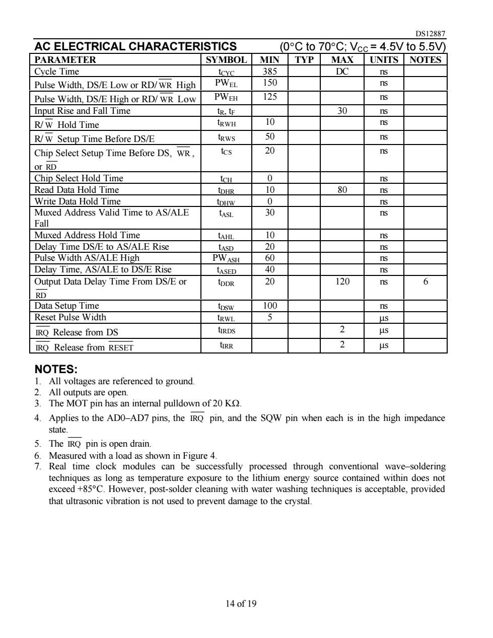
DS12887 AC ELECTRICAL CHARACTERISTICS (0C to 70C;Vcc=4.5V to 5.5V) PARAMETER SYMBOL MIN TYP MAX UNITS I NOTES Cycle Time 2R5 DC n Pulse Width,DS/E Low or RD/WR High PWEL 150 Pulse Width,DS/E High or RD/WR Low PWEH 125 s Input Rise and Fall Time tR 30 R/W Hold Time IRWH 10 R/W Setup Time Before DS/E 50 Chip Select Setup Time Before DS,WR tcs 20 s or RD Chip Select Hold Time tu 0 s Read Data Hold Time 10 80 Write Data Hold Time 0 Muxed Address valid Time to as/Ale 30 s Fall tAHL 10 20 s Pulse Width AS/ALE High 60 Delay Time,AS/ALE to DS/E Rise tASED 40 s Output Data Delay Time From DS/E or 20 120 6 etup Tin tpsw 100 s Reset Pulse Width IRWL IRQ Release from DS UIRDS 2 IRO Release from RESET UIRR 2 us NOTES: ges are referenced to ground The intemal of20K 4.Applies to the ADO-AD7 pins,the IRQ pin,and the SQW pin when each is in the high impedance state 5.The IRQ pin is open drain. 6.Measured with a load as shown in Figure 4. 7.Real time clock modules can be successfully processed through conventional wave-soldering techniques as long as tempe gy source contained within does not exceed+85°C.H ever,po ith wate washi techniques is acceptable provided 14of19DS12887 14 of 19 AC ELECTRICAL CHARACTERISTICS (0°C to 70°C; VCC = 4.5V to 5.5V) PARAMETER SYMBOL MIN TYP MAX UNITS NOTES Cycle Time tCYC 385 DC ns Pulse Width, DS/E Low or RD/ WR High PWEL 150 ns Pulse Width, DS/E High or RD/ WR Low PWEH 125 ns Input Rise and Fall Time tR, tF 30 ns R/ W Hold Time tRWH 10 ns R/ W Setup Time Before DS/E tRWS 50 ns Chip Select Setup Time Before DS, WR , or RD tCS 20 ns Chip Select Hold Time tCH 0 ns Read Data Hold Time tDHR 10 80 ns Write Data Hold Time tDHW 0 ns Muxed Address Valid Time to AS/ALE Fall tASL 30 ns Muxed Address Hold Time tAHL 10 ns Delay Time DS/E to AS/ALE Rise tASD 20 ns Pulse Width AS/ALE High PWASH 60 ns Delay Time, AS/ALE to DS/E Rise tASED 40 ns Output Data Delay Time From DS/E or RD tDDR 20 120 ns 6 Data Setup Time tDSW 100 ns Reset Pulse Width tRWL 5 ms IRQ Release from DS tIRDS 2 ms IRQ Release from RESET tIRR 2 ms NOTES: 1. All voltages are referenced to ground. 2. All outputs are open. 3. The MOT pin has an internal pulldown of 20 KW. 4. Applies to the AD0–AD7 pins, the IRQ pin, and the SQW pin when each is in the high impedance state. 5. The IRQ pin is open drain. 6. Measured with a load as shown in Figure 4. 7. Real time clock modules can be successfully processed through conventional wave–soldering techniques as long as temperature exposure to the lithium energy source contained within does not exceed +85°C. However, post-solder cleaning with water washing techniques is acceptable, provided that ultrasonic vibration is not used to prevent damage to the crystal