正在加载图片...
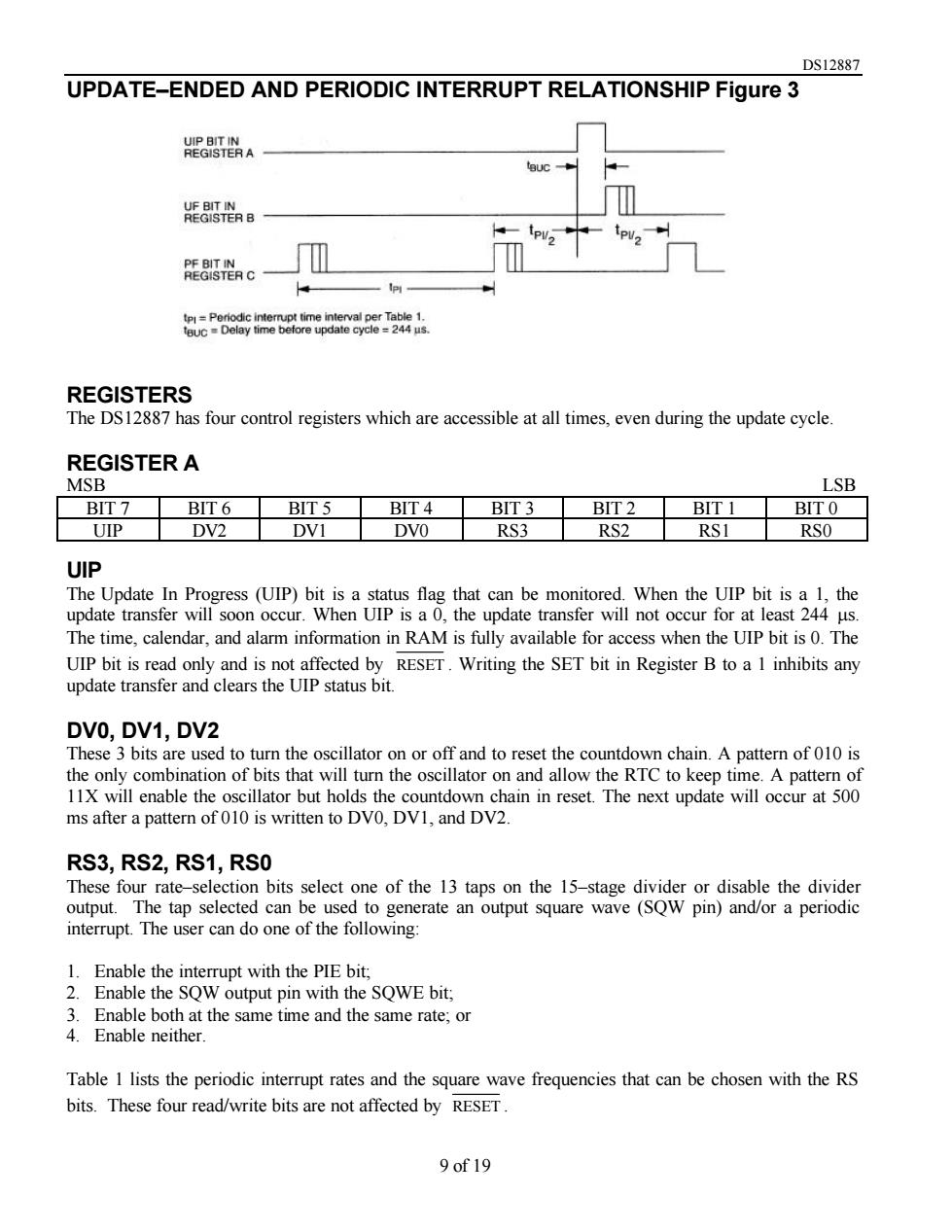
DS12887 UPDATE-ENDED AND PERIODIC INTERRUPT RELATIONSHIP Figure 3 BESSTERA REGISTER B REOISTERC acoecceopaoeeg2 REGISTERS The DS12887 has four control registers which are accessible at all times.even during the update cycle REGISTER A MSB LsB BIT7 BIT6 BIT 5 BIT4 BIT3 BIT2 BIT 1 BIT0 UIP DVI RS2 UIP The Update In Progress (UIP)bit The time,calendar,and alarm information in RAM is fully available for access when the UIP bit is 0.The afcted byEr Writing the E bit in Register B to aI inhibits any lears the UIP status DVO,DV1,DV2 These 3 bits are used to turn the oscillator on or off and to reset the countdown chain.A pattern of 010 is the only combination of bits that will turn the oscillator on and allow the RTC to keep time.A pattern of 11X will enable the oscillator but holds the countdown chain in reset.The next update will occur at 500 ms after a pattern of 010 is written to DV0,DV1,and DV2. RS3,RS2,RS1,RS0 These four rate-sel er or disable the divider output. use o generate an output square wave (SQW pin)and/or a periodic interrupt.The user can do one of the following: 1.Enable the interrupt with the PIE bit, 2.Enable the SQW output pin with the SQWE bit; 3.Enable both at the same time and the same rate;or 4.Enable neither Table 1 lists the periodic interrupt rates and the square wave frequencies that can be chosen with the RS bits.These four read/write bits are not affected by RESE 9of19 DS12887 9 of 19 UPDATE–ENDED AND PERIODIC INTERRUPT RELATIONSHIP Figure 3 REGISTERS The DS12887 has four control registers which are accessible at all times, even during the update cycle. REGISTER A MSB LSB BIT 7 BIT 6 BIT 5 BIT 4 BIT 3 BIT 2 BIT 1 BIT 0 UIP DV2 DV1 DV0 RS3 RS2 RS1 RS0 UIP The Update In Progress (UIP) bit is a status flag that can be monitored. When the UIP bit is a 1, the update transfer will soon occur. When UIP is a 0, the update transfer will not occur for at least 244 ms. The time, calendar, and alarm information in RAM is fully available for access when the UIP bit is 0. The UIP bit is read only and is not affected by RESET . Writing the SET bit in Register B to a 1 inhibits any update transfer and clears the UIP status bit. DV0, DV1, DV2 These 3 bits are used to turn the oscillator on or off and to reset the countdown chain. A pattern of 010 is the only combination of bits that will turn the oscillator on and allow the RTC to keep time. A pattern of 11X will enable the oscillator but holds the countdown chain in reset. The next update will occur at 500 ms after a pattern of 010 is written to DV0, DV1, and DV2. RS3, RS2, RS1, RS0 These four rate–selection bits select one of the 13 taps on the 15–stage divider or disable the divider output. The tap selected can be used to generate an output square wave (SQW pin) and/or a periodic interrupt. The user can do one of the following: 1. Enable the interrupt with the PIE bit; 2. Enable the SQW output pin with the SQWE bit; 3. Enable both at the same time and the same rate; or 4. Enable neither. Table 1 lists the periodic interrupt rates and the square wave frequencies that can be chosen with the RS bits. These four read/write bits are not affected by RESET