正在加载图片...
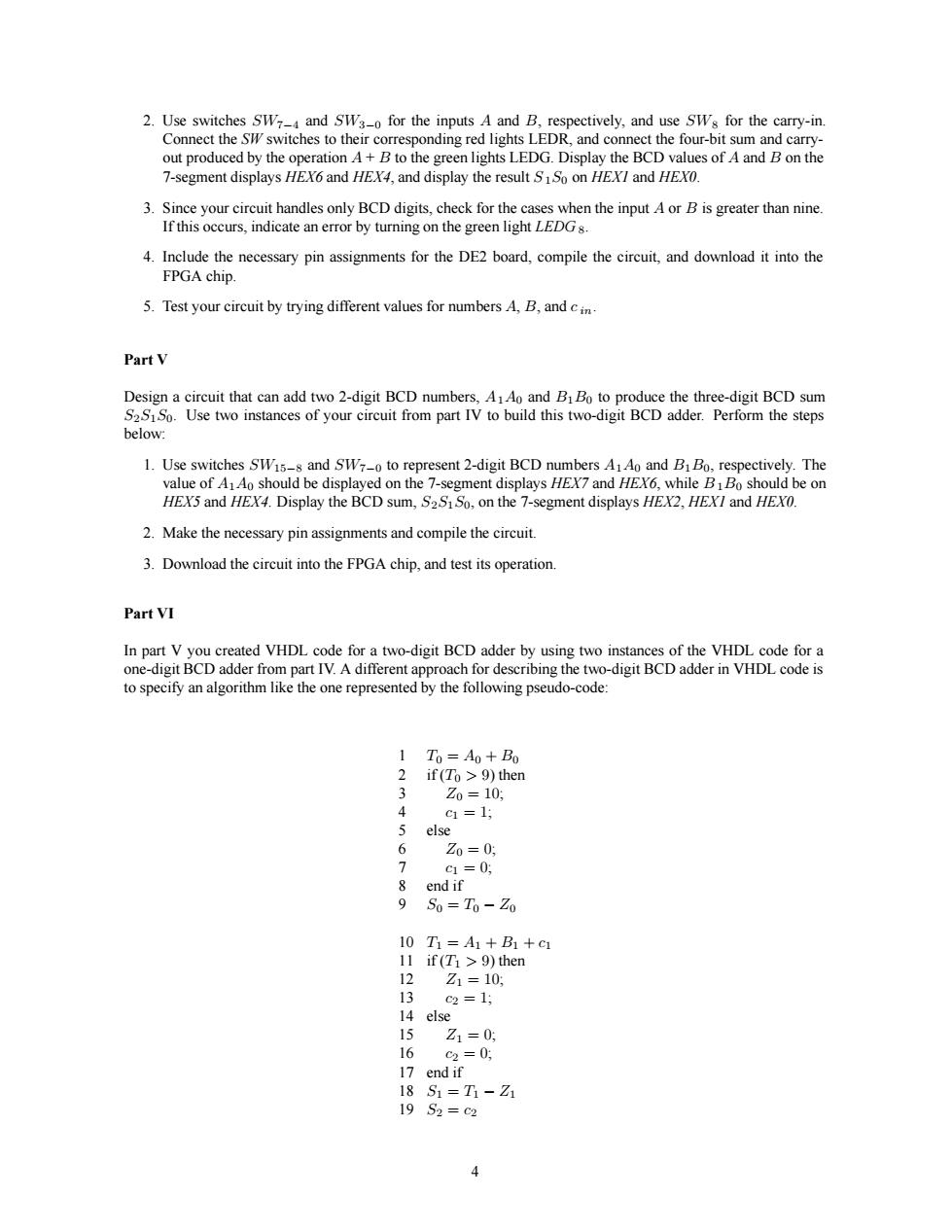
nd sw for the e Sw foe th out produced by the operation A+B to the green lights LEDG.Display the BCD values of A and B on the 7-segment displays HEX6 and HEX4,and display the result S So on HEX/and HEXO. 4.Include the necessary pin assignments for the DE2 board,compile the circuit,and download it into the FPGA chip. 5.Test your circuit by trying different values for numbers A.B.andc Part V 一设o邮 rform the steps 1 Use switches Sw nt 2 digit BCD A.Aand R.R ively.The of o should be displayed gment displays HEX7andHE6,while BBo should be on HEX5 and HEX4.Display the BCD sum,S2SSo,on the 7-segment displays HEX2,HEXI and HEX0. 2.Make the necessary pin assignments and compile the circuit. 3.Download the circuit into the FPGA chip,and test its operation PartVI In part V you created VHDL code for a two-digit BCD adder by using two instances of the VHDL code for a one-digit BCD adde one Te the tollowing code is to specity an algorithm like the one represente 1T。三A+B 2 if(To>9)then 6 Zn.=0 9 10T=A1+B+c 14 else 67 1=0 19S2=c2 2. Use switches SW7−4 and SW3−0 for the inputs A and B, respectively, and use SW8 for the carry-in. Connect the SW switches to their corresponding red lights LEDR, and connect the four-bit sum and carryout produced by the operation A + B to the green lights LEDG. Display the BCD values of A and B on the 7-segment displays HEX6 and HEX4, and display the result S1S0 on HEX1 and HEX0. 3. Since your circuit handles only BCD digits, check for the cases when the input A or B is greater than nine. If this occurs, indicate an error by turning on the green light LEDG 8. 4. Include the necessary pin assignments for the DE2 board, compile the circuit, and download it into the FPGA chip. 5. Test your circuit by trying different values for numbers A, B, and c in. Part V Design a circuit that can add two 2-digit BCD numbers, A1A0 and B1B0 to produce the three-digit BCD sum S2S1S0. Use two instances of your circuit from part IV to build this two-digit BCD adder. Perform the steps below: 1. Use switches SW15−8 and SW7−0 to represent 2-digit BCD numbers A1A0 and B1B0, respectively. The value of A1A0 should be displayed on the 7-segment displays HEX7 and HEX6, while B1B0 should be on HEX5 and HEX4. Display the BCD sum, S2S1S0, on the 7-segment displays HEX2, HEX1 and HEX0. 2. Make the necessary pin assignments and compile the circuit. 3. Download the circuit into the FPGA chip, and test its operation. Part VI In part V you created VHDL code for a two-digit BCD adder by using two instances of the VHDL code for a one-digit BCD adder from part IV. A different approach for describing the two-digit BCD adder in VHDL code is to specify an algorithm like the one represented by the following pseudo-code: 1 T0 = A0 + B0 2 if (T0 > 9) then 3 Z0 = 10; 4 c1 = 1; 5 else 6 Z0 = 0; 7 c1 = 0; 8 end if 9 S0 = T0 − Z0 10 T1 = A1 + B1 + c1 11 if (T1 > 9) then 12 Z1 = 10; 13 c2 = 1; 14 else 15 Z1 = 0; 16 c2 = 0; 17 end if 18 S1 = T1 − Z1 19 S2 = c2 4