正在加载图片...
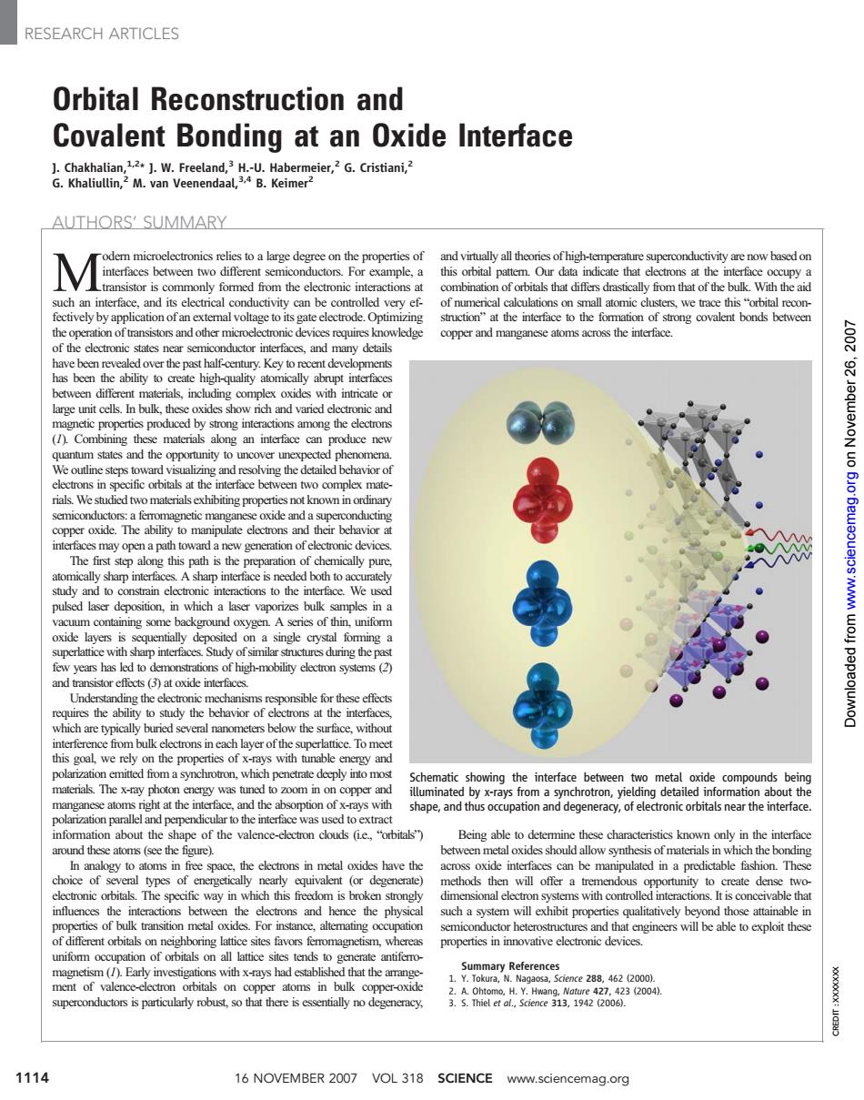
RESEARCH ARTICLES Orbital Reconstruction and Covalent Bonding at an Oxide Interface J.Chakhalian,12*]W.Freeland,3 H.-U.Habermeier,2 G.Cristiani,2 G.Khaliullin,2 M.van Veenendaal,3.4 B.Keimer2 AUTHORS'SUMMARY -odem microelectronics relies to a large degree on the properties of and virtually all theories ofhigh-temperature superconductivity are now based on interfaces between two different semiconductors.For example,a this orbital pattem.Our data indicate that electrons at the interface occupy a transistor is commonly formed from the electronic interactions at combination of orbitals that differs drastically from that of the bulk.With the aid such an interface,and its electrical conductivity can be controlled very ef- of numerical calculations on small atomic clusters,we trace this"orbital recon- fectively by application of an external voltage to its gate electrode.Optimizing struction"at the interface to the formation of strong covalent bonds between the operation oftransistors and other microelectronic devices requires knowledge copper and manganese atoms across the interface. of the electronic states near semiconductor interfaces,and many details 1000 have been revealed over the past half-century.Key to recent developments has been the ability to create high-quality atomically abrupt interfaces between different materials,including complex oxides with intricate or large unit cells.In bulk,these oxides show rich and varied electronic and magnetic properties produced by strong interactions among the electrons (1).Combining these materials along an interface can produce new quantum states and the opportunity to uncover unexpected phenomena. We outline steps toward visualizing and resolving the detailed behavior of electrons in specific orbitals at the interface between two complex mate- rials.We studied two materials exhibiting properties not known in ordinary semiconductors:a ferromagnetic manganese oxide and a superconducting copper oxide.The ability to manipulate electrons and their behavior at interfaces may open a path toward a new generation of electronic devices. The first step along this path is the preparation of chemically pure, atomically sharp interfaces.A sharp interface is needed both to accurately study and to constrain electronic interactions to the interface.We used pulsed laser deposition,in which a laser vaporizes bullk samples in a vacuum containing some background oxygen.A series of thin,uniform oxide layers is sequentially deposited on a single crystal forming a superlattice with sharp interfaces.Study of similar structures during the past few years has led to demonstrations of high-mobility electron systems (2) and transistor effects (3)at oxide interfaces. Understanding the electronic mechanisms responsible for these effects requires the ability to study the behavior of electrons at the interfaces, which are typically buried several nanometers below the surface,without interference from bulk electrons in each layer of the superlattice.To meet this goal,we rely on the properties of x-rays with tunable energy and polarization emitted from a synchrotron,which penetrate deeply into most Schematic showing the interface between two metal oxide compounds being materials.The x-ray photon energy was tuned to zoom in on copper and illuminated by x-rays from a synchrotron,yielding detailed information about the manganese atoms right at the interface,and the absorption of x-rays with shape,and thus occupation and degeneracy,of electronic orbitals near the interface. polarization parallel and perpendicular to the interface was used to extract information about the shape of the valence-electron clouds (ie.,"orbitals") Being able to determine these characteristics known only in the interface around these atoms(see the figure). between metal oxides should allow synthesis of materials in which the bonding In analogy to atoms in free space,the electrons in metal oxides have the across oxide interfaces can be manipulated in a predictable fashion.These choice of several types of energetically nearly equivalent (or degenerate) methods then will offer a tremendous opportunity to create dense two- electronic orbitals.The specific way in which this freedom is broken strongly dimensional electron systems with controlled interactions.It is conceivable that influences the interactions between the electrons and hence the physical such a system will exhibit properties qualitatively beyond those attainable in properties of bulk transition metal oxides.For instance,altemating occupation semiconductor heterostructures and that engineers will be able to exploit these of different orbitals on neighboring lattice sites favors feromagnetism,whereas properties in innovative electronic devices. unifomm occupation of orbitals on all lattice sites tends to generate antiferro- magnetism().Early investigations with x-rays had established that the arrange- Summary References 1.Y.Tokura,N.Nagaosa,Science 288,462 (2000). ment of valence-electron orbitals on copper atoms in bulk copper-oxide 2.A.Ohtomo,H.Y.Hwang,Nature 427,423 (2004). superconductors is particularly robust,so that there is essentially no degeneracy. 3.S.Thiel et al.,Science 313,1942 (2006). 1114 16 NOVEMBER 2007 VOL 318 SCIENCE www.sciencemag.orgOrbital Reconstruction and Covalent Bonding at an Oxide Interface J. Chakhalian,1,2* J. W. Freeland,3 H.-U. Habermeier,2 G. Cristiani,2 G. Khaliullin,2 M. van Veenendaal,3,4 B. Keimer2 AUTHORS’ SUMMARY Modern microelectronics relies to a large degree on the properties of interfaces between two different semiconductors. For example, a transistor is commonly formed from the electronic interactions at such an interface, and its electrical conductivity can be controlled very effectively by application of an external voltage to its gate electrode. Optimizing the operation of transistors and other microelectronic devices requires knowledge of the electronic states near semiconductor interfaces, and many details have been revealed over the past half-century. Key to recent developments has been the ability to create high-quality atomically abrupt interfaces between different materials, including complex oxides with intricate or large unit cells. In bulk, these oxides show rich and varied electronic and magnetic properties produced by strong interactions among the electrons (1). Combining these materials along an interface can produce new quantum states and the opportunity to uncover unexpected phenomena. We outline steps toward visualizing and resolving the detailed behavior of electrons in specific orbitals at the interface between two complex materials.We studied two materials exhibiting properties not known in ordinary semiconductors: a ferromagnetic manganese oxide and a superconducting copper oxide. The ability to manipulate electrons and their behavior at interfaces may open a path toward a new generation of electronic devices. The first step along this path is the preparation of chemically pure, atomically sharp interfaces. A sharp interface is needed both to accurately study and to constrain electronic interactions to the interface. We used pulsed laser deposition, in which a laser vaporizes bulk samples in a vacuum containing some background oxygen. A series of thin, uniform oxide layers is sequentially deposited on a single crystal forming a superlattice with sharp interfaces. Study of similar structures during the past few years has led to demonstrations of high-mobility electron systems (2) and transistor effects (3) at oxide interfaces. Understanding the electronic mechanisms responsible for these effects requires the ability to study the behavior of electrons at the interfaces, which are typically buried several nanometers below the surface, without interference from bulk electrons in each layer of the superlattice. To meet this goal, we rely on the properties of x-rays with tunable energy and polarization emitted from a synchrotron, which penetrate deeply into most materials. The x-ray photon energy was tuned to zoom in on copper and manganese atoms right at the interface, and the absorption of x-rays with polarization parallel and perpendicular to the interface was used to extract information about the shape of the valence-electron clouds (i.e., “orbitals”) around these atoms (see the figure). In analogy to atoms in free space, the electrons in metal oxides have the choice of several types of energetically nearly equivalent (or degenerate) electronic orbitals. The specific way in which this freedom is broken strongly influences the interactions between the electrons and hence the physical properties of bulk transition metal oxides. For instance, alternating occupation of different orbitals on neighboring lattice sites favors ferromagnetism, whereas uniform occupation of orbitals on all lattice sites tends to generate antiferromagnetism (1). Early investigations with x-rays had established that the arrangement of valence-electron orbitals on copper atoms in bulk copper-oxide superconductors is particularly robust, so that there is essentially no degeneracy, and virtually all theories of high-temperature superconductivity are now based on this orbital pattern. Our data indicate that electrons at the interface occupy a combination of orbitals that differs drastically from that of the bulk. With the aid of numerical calculations on small atomic clusters, we trace this “orbital reconstruction” at the interface to the formation of strong covalent bonds between copper and manganese atoms across the interface. Being able to determine these characteristics known only in the interface between metal oxides should allow synthesis of materials in which the bonding across oxide interfaces can be manipulated in a predictable fashion. These methods then will offer a tremendous opportunity to create dense twodimensional electron systems with controlled interactions. It is conceivable that such a system will exhibit properties qualitatively beyond those attainable in semiconductor heterostructures and that engineers will be able to exploit these properties in innovative electronic devices. Summary References 1. Y. Tokura, N. Nagaosa, Science 288, 462 (2000). 2. A. Ohtomo, H. Y. Hwang, Nature 427, 423 (2004). 3. S. Thiel et al., Science 313, 1942 (2006). Schematic showing the interface between two metal oxide compounds being illuminated by x-rays from a synchrotron, yielding detailed information about the shape, and thus occupation and degeneracy, of electronic orbitals near the interface. 1114 16 NOVEMBER 2007 VOL 318 SCIENCE www.sciencemag.org CREDIT : XXXXXXX RESEARCH ARTICLES on November 26, 2007 www.sciencemag.org Downloaded from