正在加载图片...
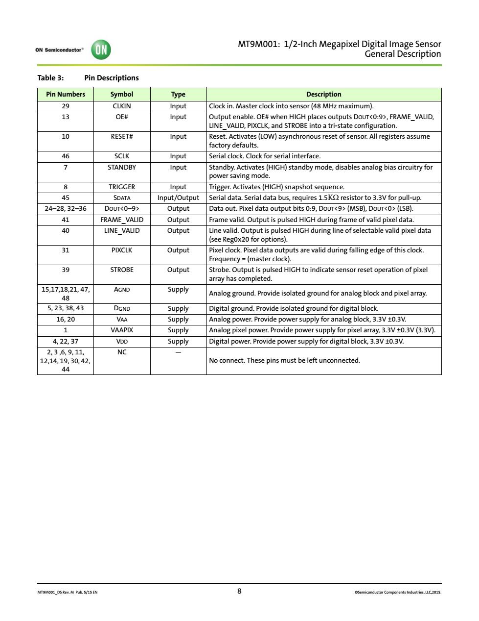
O① MT9Mo1:1/21nchMegapdD2iagm8eSto Table3: Pin Descriptions Pin Numbers Symbol Type Description 29 CLKIN Input Clock in.Master clock into sensor(48 MHz maximum). 13 OE# Input 10 RESET# Input Reset.Activates (LW)asynchronous reset of sensor.All registers assume 6 Input clockClock for serial interface. STANDBY Input EtndpytRtgmGWsandboymodedablesanaogbiasccutyfor TRIGGER rigger.Activates(HIGH)snapshot sequence. 45 SDATA tput adata.Serial data bus res 1.5KQ istor to 3.3V fo ull-up 24-28,32-36 ata out D R) 0T9 (MS FRAME VALID data outp during fran me ofv d pix LINE _VAUD Output aeRagdoigr5pmsdHGHdunglimeofseectabievaidpweldhta PIXCLK Output 39 STROBE Output Strobe.Output is pulsed HIGH to indicate sensor reset operation of pixel array has completed. 517247 AGND Supply Anaog ground.Provide isolated ground for ana block and pixel array. 5,23,38,43 Supp igital ground.Provide isolatedground for digital block. 16,20 ock,3.3V+0.3V. VAAPIX Supp吵 nalog pixel power powe upply for 3.3V0.3V3.3 4,22,37 Supply Digital power.Provide power supply for digital block3.3V3V. No connect.These pins must be left unconnected. M hS EN MT9M001_DS Rev. M Pub. 5/15 EN 8 ©Semiconductor Components Industries, LLC,2015. MT9M001: 1/2-Inch Megapixel Digital Image Sensor General Description Table 3: Pin Descriptions Pin Numbers Symbol Type Description 29 CLKIN Input Clock in. Master clock into sensor (48 MHz maximum). 13 OE# Input Output enable. OE# when HIGH places outputs DOUT<0:9>, FRAME_VALID, LINE_VALID, PIXCLK, and STROBE into a tri-state configuration. 10 RESET# Input Reset. Activates (LOW) asynchronous reset of sensor. All registers assume factory defaults. 46 SCLK Input Serial clock. Clock for serial interface. 7 STANDBY Input Standby. Activates (HIGH) standby mode, disables analog bias circuitry for power saving mode. 8 TRIGGER Input Trigger. Activates (HIGH) snapshot sequence. 45 SDATA Input/Output Serial data. Serial data bus, requires 1.5K resistor to 3.3V for pull-up. 24–28, 32–36 DOUT<0–9> Output Data out. Pixel data output bits 0:9, DOUT<9> (MSB), DOUT<0> (LSB). 41 FRAME_VALID Output Frame valid. Output is pulsed HIGH during frame of valid pixel data. 40 LINE_VALID Output Line valid. Output is pulsed HIGH during line of selectable valid pixel data (see Reg0x20 for options). 31 PIXCLK Output Pixel clock. Pixel data outputs are valid during falling edge of this clock. Frequency = (master clock). 39 STROBE Output Strobe. Output is pulsed HIGH to indicate sensor reset operation of pixel array has completed. 15,17,18,21, 47, 48 AGND Supply Analog ground. Provide isolated ground for analog block and pixel array. 5, 23, 38, 43 DGND Supply Digital ground. Provide isolated ground for digital block. 16, 20 VAA Supply Analog power. Provide power supply for analog block, 3.3V ±0.3V. 1 VAAPIX Supply Analog pixel power. Provide power supply for pixel array, 3.3V ±0.3V (3.3V). 4, 22, 37 VDD Supply Digital power. Provide power supply for digital block, 3.3V ±0.3V. 2, 3 ,6, 9, 11, 12,14, 19, 30, 42, 44 NC — No connect. These pins must be left unconnected