正在加载图片...
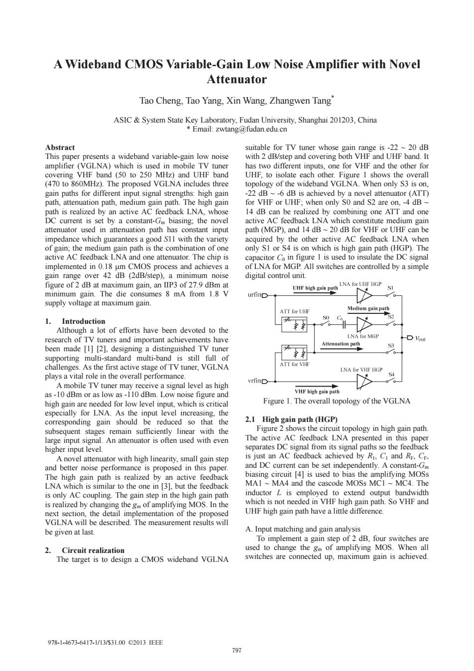
A Wideband CMOS Variable-Gain Low Noise Amplifier with Novel Attenuator Tao Cheng,Tao Yang,Xin Wang,Zhangwen Tang ASIC System State Key Laboratory,Fudan University,Shanghai 201203,China Email:zwtang@fudan.edu.cn Abstract suitable for TV tuner whose gain range is-22 ~20 dB This paper presents a wideband variable-gain low noise with 2 dB/step and covering both VHF and UHF band.It amplifier (VGLNA)which is used in mobile TV tuner has two different inputs,one for VHF and the other for covering VHF band (50 to 250 MHz)and UHF band UHF,to isolate each other.Figure I shows the overall (470 to 860MHz).The proposed VGLNA includes three topology of the wideband VGLNA.When only S3 is on, gain paths for different input signal strengths:high gain -22 dB ~-6 dB is achieved by a novel attenuator (ATT) path,attenuation path,medium gain path.The high gain for VHF or UHF:when only S0 and S2 are on,-4 dB path is realized by an active AC feedback LNA,whose 14 dB can be realized by combining one ATT and one DC current is set by a constant-Gm biasing;the novel active AC feedback LNA which constitute medium gain attenuator used in attenuation path has constant input path(MGP),and 14 dB~20 dB for VHF or UHF can be impedance which guarantees a good S11 with the variety acquired by the other active AC feedback LNA when of gain;the medium gain path is the combination of one only SI or S4 is on which is high gain path(HGP).The active AC feedback LNA and one attenuator.The chip is capacitor Co in figure 1 is used to insulate the DC signal implemented in 0.18 um CMOS process and achieves a of LNA for MGP.All switches are controlled by a simple gain range over 42 dB (2dB/step),a minimum noise digital control unit. figure of 2 dB at maximum gain,an IIP3 of 27.9 dBm at LNA for UHF HGP UHF high gain path minimum gain.The die consumes 8 mA from 1.8 V urfinD supply voltage at maximum gain. ATT for UHF Medium gain path 1.Introduction Although a lot of efforts have been devoted to the research of TV tuners and important achievements have LNA for MGP been made [1][2],designing a distinguished TV tuner Attenuation path supporting multi-standard multi-band is still full of challenges.As the first active stage of TV tuner,VGLNA ATT for VHF LNA for VHF HGP plays a vital role in the overall performance. A mobile TV tuner may receive a signal level as high vrfinD as-10 dBm or as low as-110 dBm.Low noise figure and VHF high gain path high gain are needed for low level input,which is critical Figure 1.The overall topology of the VGLNA especially for LNA.As the input level increasing,the corresponding gain should be reduced so that the 2.1 High gain path(HGP) subsequent stages remain sufficiently linear with the Figure 2 shows the circuit topology in high gain path large input signal.An attenuator is often used with even The active AC feedback LNA presented in this paper higher input level. separates DC signal from its signal paths so the feedback A novel attenuator with high linearity,small gain step is just an AC feedback achieved by Ri,Ci and Rr,Cr, and better noise performance is proposed in this paper. and DC current can be set independently.A constant-Gm The high gain path is realized by an active feedback biasing circuit [4]is used to bias the amplifying MOSs LNA which is similar to the one in [31.but the feedback MAI ~MA4 and the cascode MOSs MC1 MC4.The is only AC coupling.The gain step in the high gain path inductor L is employed to extend output bandwidth is realized by changing the gm of amplifying MOS.In the which is not needed in VHF high gain path.So VHF and next section,the detail implementation of the proposed UHF high gain path have a little difference. VGLNA will be described.The measurement results will be given at last. A.Input matching and gain analysis To implement a gain step of 2 dB,four switches are Circuit realization used to change the gm of amplifying MOS.When all The target is to design a CMOS wideband VGLNA switches are connected up,maximum gain is achieved. 978-1-4673-6417-1/13/$31.00C2013IEEE 797A Wideband CMOS Variable-Gain Low Noise Amplifier with Novel Attenuator Tao Cheng, Tao Yang, Xin Wang, Zhangwen Tang* ASIC & System State Key Laboratory, Fudan University, Shanghai 201203, China * Email: zwtang@fudan.edu.cn Abstract This paper presents a wideband variable-gain low noise amplifier (VGLNA) which is used in mobile TV tuner covering VHF band (50 to 250 MHz) and UHF band (470 to 860MHz). The proposed VGLNA includes three gain paths for different input signal strengths: high gain path, attenuation path, medium gain path. The high gain path is realized by an active AC feedback LNA, whose DC current is set by a constant-Gm biasing; the novel attenuator used in attenuation path has constant input impedance which guarantees a good S11 with the variety of gain; the medium gain path is the combination of one active AC feedback LNA and one attenuator. The chip is implemented in 0.18 ȝm CMOS process and achieves a gain range over 42 dB (2dB/step), a minimum noise figure of 2 dB at maximum gain, an IIP3 of 27.9 dBm at minimum gain. The die consumes 8 mA from 1.8 V supply voltage at maximum gain. 1. Introduction Although a lot of efforts have been devoted to the research of TV tuners and important achievements have been made [1] [2], designing a distinguished TV tuner supporting multi-standard multi-band is still full of challenges. As the first active stage of TV tuner, VGLNA plays a vital role in the overall performance. A mobile TV tuner may receive a signal level as high as -10 dBm or as low as -110 dBm. Low noise figure and high gain are needed for low level input, which is critical especially for LNA. As the input level increasing, the corresponding gain should be reduced so that the subsequent stages remain sufficiently linear with the large input signal. An attenuator is often used with even higher input level. A novel attenuator with high linearity, small gain step and better noise performance is proposed in this paper. The high gain path is realized by an active feedback LNA which is similar to the one in [3], but the feedback is only AC coupling. The gain step in the high gain path is realized by changing the gm of amplifying MOS. In the next section, the detail implementation of the proposed VGLNA will be described. The measurement results will be given at last. 2. Circuit realization The target is to design a CMOS wideband VGLNA suitable for TV tuner whose gain range is -22 ~ 20 dB with 2 dB/step and covering both VHF and UHF band. It has two different inputs, one for VHF and the other for UHF, to isolate each other. Figure 1 shows the overall topology of the wideband VGLNA. When only S3 is on, -22 dB ~ -6 dB is achieved by a novel attenuator (ATT) for VHF or UHF; when only S0 and S2 are on, -4 dB ~ 14 dB can be realized by combining one ATT and one active AC feedback LNA which constitute medium gain path (MGP), and 14 dB ~ 20 dB for VHF or UHF can be acquired by the other active AC feedback LNA when only S1 or S4 is on which is high gain path (HGP). The capacitor C0 in figure 1 is used to insulate the DC signal of LNA for MGP. All switches are controlled by a simple digital control unit. Figure 1. The overall topology of the VGLNA 2.1 High gain path (HGP) Figure 2 shows the circuit topology in high gain path. The active AC feedback LNA presented in this paper separates DC signal from its signal paths so the feedback is just an AC feedback achieved by R1, C1 and RF, CF, and DC current can be set independently. A constant-Gm biasing circuit [4] is used to bias the amplifying MOSs MA1 ~ MA4 and the cascode MOSs MC1 ~ MC4. The inductor L is employed to extend output bandwidth which is not needed in VHF high gain path. So VHF and UHF high gain path have a little difference. A. Input matching and gain analysis To implement a gain step of 2 dB, four switches are used to change the gm of amplifying MOS. When all switches are connected up, maximum gain is achieved. 978-1-4673-6417-1/13/$31.00 ©2013 IEEE 797