正在加载图片...
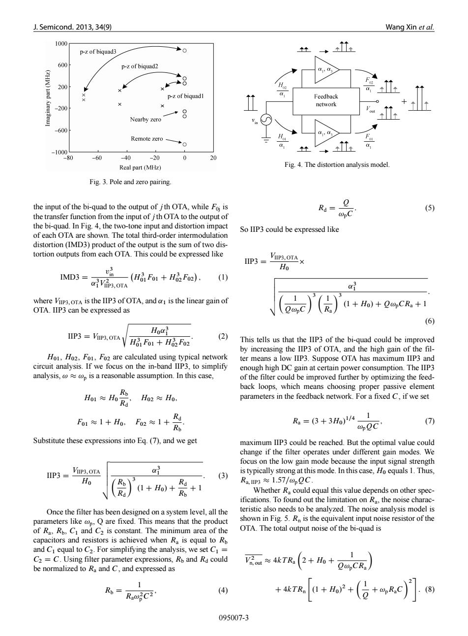
J.Semicond.2013,34(9) Wang Xin et al. 1000 p-z of biquad3 600 p-z of biquad2 1,g +8 200 复 p-z of biquadl Feedback -200 network Nearby zero *8 -600 1,3 Remote zero *0 -100 80 -60 -40 -20 0 20 Real part (MHz) Fig.4.The distortion analysis model. Fig.3.Pole and zero pairing. the input of the bi-quad to the output of jth OTA,while Foi is Rd= (5) the transfer function from the input of jth OTA to the output of WpC the bi-quad.In Fig.4,the two-tone input and distortion impact So IIP3 could be expressed like of each OTA are shown.The total third-order intermodulation distortion(IMD3)product of the output is the sum of two dis- tortion outputs from each OTA.This could be expressed like IIP3= V1P3,oTA× 唱 Ho IMD3= —(H61Fo1+H2Fo2). VIP3.OTA (1) ai where ViP3,oTA is the IIP3 of OTA,and is the linear gain of (1+Ho)+QopCRa+1 OTA.IIP3 can be expressed as R (6) IIP3 VuP3.OTA Hoa (2) Ho1 Fo1+Ho2 Fo2 This tells us that the IIP3 of the bi-quad could be improved by increasing the IIP3 of OTA,and the high gain of the fil- Ho1,Ho2,Fo1,Fo2 are calculated using typical network ter means a low IIP3.Suppose OTA has maximum IIP3 and circuit analysis.If we focus on the in-band IIP3,to simplify enough high DC gain at certain power consumption.The IIP3 analysis,p is a reasonable assumption.In this case, of the filter could be improved further by optimizing the feed- back loops,which means choosing proper passive element Ho1≈H0R b Ho2≈Ho, parameters in the feedback network.For a fixed C,if we set Fo1≈1+Ho, F2≈1+ Rb Ra=(3+3Ho)/41 @pOc (7) Substitute these expressions into Eq.(7),and we get maximum IIP3 could be reached.But the optimal value could change if the filter operates under different gain modes.We focus on the low gain mode because the input signal strength IIP3 ViIP3,OTA a ⊙ (3) is typically strong at this mode.In this case,Ho equals 1.Thus, R Ra Ra,p3≈1.57/op0C. (1+Ho)+ +1 Rb Whether Ra could equal this value depends on other spec- ifications.To found out the limitation on Ra,the noise charac- Once the filter has been designed on a system level,all the teristic also needs to be analyzed.The noise analysis model is parameters like p,Q are fixed.This means that the product shown in Fig.5.Rn is the equivalent input noise resistor of the of Ra,Rp,Ci and C2 is constant.The minimum area of the OTA.The total output noise of the bi-quad is capacitors and resistors is achieved when Ra is equal to Rp and Ci equal to C2.For simplifying the analysis,we set C1= C2=C.Using filter parameter expressions,Ro and Ra could be normalized to Ra and C,and expressed as ≈4kTR(2++QCR 1 Rb= RawC2' (4) +++(合+门 095007-3J. Semicond. 2013, 34(9) Wang Xin et al. Fig. 3. Pole and zero pairing. the input of the bi-quad to the output of j th OTA, while F0j is the transfer function from the input of j th OTA to the output of the bi-quad. In Fig. 4, the two-tone input and distortion impact of each OTA are shown. The total third-order intermodulation distortion (IMD3) product of the output is the sum of two distortion outputs from each OTA. This could be expressed like IMD3 D v 3 in ˛ 3 1V 2 IIP3; OTA H3 01F01 C H3 02F02 ; (1) where VIIP3; OTA is the IIP3 of OTA, and ˛1 is the linear gain of OTA. IIP3 can be expressed as IIP3 D VIIP3; OTAs H0˛ 3 1 H3 01F01 C H3 02F02 : (2) H01, H02, F01, F02 are calculated using typical network circuit analysis. If we focus on the in-band IIP3, to simplify analysis, ! !p is a reasonable assumption. In this case, H01 H0 Rb Rd ; H02 H0; F01 1 C H0; F02 1 C Rd Rb : Substitute these expressions into Eq. (7), and we get IIP3 D VIIP3; OTA H0 vuuuut ˛ 3 1 Rb Rd 3 .1 C H0/ C Rd Rb C 1 : (3) Once the filter has been designed on a system level, all the parameters like !p, Q are fixed. This means that the product of Ra, Rb, C1 and C2 is constant. The minimum area of the capacitors and resistors is achieved when Ra is equal to Rb and C1 equal to C2. For simplifying the analysis, we set C1 D C2 D C. Using filter parameter expressions, Rb and Rd could be normalized to Ra and C, and expressed as Rb D 1 Ra!2 pC2 ; (4) Fig. 4. The distortion analysis model. Rd D Q !pC : (5) So IIP3 could be expressed like IIP3 D VIIP3; OTA H0 vuuuut ˛ 3 1 1 Q!pC 3 1 Ra 3 .1 C H0/ C Q!pCRa C 1 : (6) This tells us that the IIP3 of the bi-quad could be improved by increasing the IIP3 of OTA, and the high gain of the filter means a low IIP3. Suppose OTA has maximum IIP3 and enough high DC gain at certain power consumption. The IIP3 of the filter could be improved further by optimizing the feedback loops, which means choosing proper passive element parameters in the feedback network. For a fixed C, if we set Ra D .3 C 3H0/ 1=4 1 !pQC ; (7) maximum IIP3 could be reached. But the optimal value could change if the filter operates under different gain modes. We focus on the low gain mode because the input signal strength is typically strong at this mode. In this case, H0 equals 1. Thus, Ra; IIP3 1:57=!pQC. Whether Ra could equal this value depends on other specifications. To found out the limitation on Ra, the noise characteristic also needs to be analyzed. The noise analysis model is shown in Fig. 5. Rn is the equivalent input noise resistor of the OTA. The total output noise of the bi-quad is V 2 n; out 4kTRa 2 C H0 C 1 Q!pCRa C 4kTRn " .1 C H0/ 2 C 1 Q C !pRaC 2 # : (8) 095007-3�