正在加载图片...
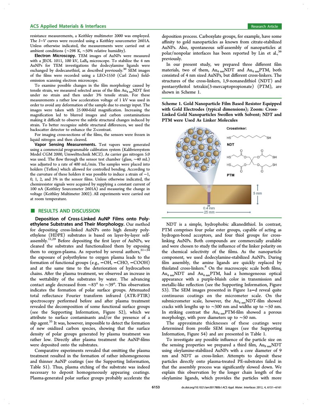
ACS Applied Materials Interfaces Research Article resistance measurements,a Keithley multimeter 2000 was employed. deposition process.Carboxylate groups,for example,have some The I-V curves were recorded using a Keithley sourcemeter 2601A. affinity to gold nanoparticles as known from citrate-stabilized Unless otherwise indicated,the measurements were carried out at AuNPs.Also,spontaneous self-assembly of nanoparticles at ambient conditions (~298 K,~50%relative humidity). Electron Microscopy.TEM images of AuNPs were measured polar/nonpolar interfaces has been reported by Lin et al.36 with a JEOL 1011,100 kV,LaBs microscope.To stabilize the 4 nm previously. AuNPs for TEM investigations the dodecylamine ligands were In our present study,we prepared three different film exchanged by dodecanethiol,as described previously.3 SEM images materials,two of them,AunmNDT and Au nmPTM,both of the films were recorded using a LEO-1550 (Carl Zeiss)field. consisted of 4 nm sized AuNPs,but different cross-linkers.The emission scanning electron microscope structures of the cross-linkers,1,9-nonanedithiol (NDT)and To examine possible changes in the film morphology caused by pentaerythritol tetrakis(3-mercaptopropionate)(PTM),are tensile strain,we measured selected areas of the film AumNDT first shown in Scheme 1. under no strain and then under 3%tensile strain.For these measurements a rather low acceleration voltage of 1 kV was used in order to avoid any deformation of the sample due to energy input.The Scheme 1.Gold Nanoparticle Film Based Resistor Equipped images were taken with 25 000-fold magnification.Increasing the with Gold Electrodes(typical dimensions);Zoom:Cross- magnification led to blurred images and carbon contaminations Linked Gold Nanoparticles Swollen with Solvent;NDT and making it difficult to observe the subtle structural changes induced by PTM were Used As Linker Molecules strain.To better recognize subtle structural differences,we used the backscatter detector to enhance the Z-contrast. Crosslinker For imaging cross-sections of the films,the sensors were frozen in HS SH liquid nitrogen and then cleaved. Vapor Sensing Measurements.Test vapors were generated NDT using a commercial programmable calibration system (Kalibriersystem Model CGM 2000,Umwelttechnik MCZ).As carrier gas nitrogen 5.0 was used.The flow through the sensor test chamber (glass,~40 mL) was adjusted to a rate of 400 mL/min.The samples were placed into holders (Teflon)which allowed for controlled bending.According to the curvature of these holders it was possible to induce a strain of-1, PTM 0,1,2,and 3%in the sensor films.Unless otherwise indicated,the chemiresistor signals were acquired by supplying a constant current of 100 nA (Keithley Sourcemeter 2601A)and measuring the change in voltage (Keithley Multimeter 2002).All experiments were carried out at room temperature. RESULTS AND DISCUSSION 25 mm Deposition of Cross-Linked AuNP Films onto Poly- ethylene Substrates and Their Morphology.Our method NDT is a simple,hydrophobic alkanedithiol.In contrast, for depositing cross-linked AuNPs onto high density poly- PTM comprises four polar ester groups,capable of acting as ethylene (HDPE)substrates is based on layer-by-layer self- hydrogen-bond acceptors,and four thiol groups for cross- assembly.Before depositing the first layer of AuNPs,we linking AuNPs.Both compounds are commercially available opupmana and were chosen to study the influence of the linker polarity on the chemical selectivity of the films.As the nanoparticle the exposure of polyethylene to oxygen plasma leads to the component,we used dodecylamine-stabilized AuNPs.During formation of functional groups(e.g,-OH,-CHO,-COOH) film assembly,the amine ligands are quickly replaced by and at the same time to the deterioration of hydrocarbon thiolated cross-linkers.On the macroscopic scale both films, chains.After the plasma treatment,we observed an increase in AumNDT and AunmPTM,had a homogeneous optical the wettability of the substrates by water.The advancing appearance with a purple-bluish color in transmission and contact angle decreased from ~83 to ~39.This observation metallic-like reflection(see the Supporting Information,Figure indicates the formation of polar surface groups.Attenuated S3).The SEM images presented in Figure 1a-d reveal quite total reflectance Fourier transform infrared (ATR-FTIR) continuous coatings on the micrometer scale.On the spectroscopy performed before and after plasma treatment submicrometer scale,however,the AuNDT-film showed revealed the decomposition of some functional surface groups cracks with lengths up to ~300 nm and widths up to ~50 nm. (see the Supporting Information,Figure S2),which we In striking contrast the Aus amPTM-film showed a porous attribute to surface contaminants and/or the presence of a morphology,with pore diameters up to ~50 nm. slip agent.s It was,however,impossible to detect the formation The approximate thicknesses of these coatings were of new oxidized carbon species,showing that the surface determined from profile SEM images (see the Supporting density of polar groups generated by plasma treatment was Information,Figure S4)and are presented in Table 1. rather low.Directly after plasma treatment the AuNP-films To investigate any possible influence of the particle size on were deposited onto the substrates. the sensing properties we prepared a third film,AumNDT Comparative experiments revealed that omitting the plasma using oleylamine-stabilized AuNPs with a core diameter of 9 treatment resulted in the formation of rather inhomogeneous nm and NDT as cross-linker.Attempts to deposit these and thinner AuNP coatings (see the Supporting Information, particles directly onto plasma-treated PE-substrates failed in Table S1).Thus,plasma etching of the substrate was indeed that the assembly process was significantly slowed down.We necessary to deposit homogeneously appearing coatings. explain this observation by the longer chain length of the Plasma-generated polar surface groups probably accelerate the oleylamine ligands,which provides the particles with more 6153 dx.doLorg/10.1021/am301780bl ACS Appl.Mater.Interfaces 2012,4,6151-6161resistance measurements, a Keithley multimeter 2000 was employed. The I−V curves were recorded using a Keithley sourcemeter 2601A. Unless otherwise indicated, the measurements were carried out at ambient conditions (∼298 K, ∼50% relative humidity). Electron Microscopy. TEM images of AuNPs were measured with a JEOL 1011, 100 kV, LaB6 microscope. To stabilize the 4 nm AuNPs for TEM investigations the dodecylamine ligands were exchanged by dodecanethiol, as described previously.30 SEM images of the films were recorded using a LEO-1550 (Carl Zeiss) fieldemission scanning electron microscope. To examine possible changes in the film morphology caused by tensile strain, we measured selected areas of the film Au4 nmNDT first under no strain and then under 3% tensile strain. For these measurements a rather low acceleration voltage of 1 kV was used in order to avoid any deformation of the sample due to energy input. The images were taken with 25 000-fold magnification. Increasing the magnification led to blurred images and carbon contaminations making it difficult to observe the subtle structural changes induced by strain. To better recognize subtle structural differences, we used the backscatter detector to enhance the Z-contrast. For imaging cross-sections of the films, the sensors were frozen in liquid nitrogen and then cleaved. Vapor Sensing Measurements. Test vapors were generated using a commercial programmable calibration system (Kalibriersystem Model CGM 2000, Umwelttechnik MCZ). As carrier gas nitrogen 5.0 was used. The flow through the sensor test chamber (glass, ∼40 mL) was adjusted to a rate of 400 mL/min. The samples were placed into holders (Teflon) which allowed for controlled bending. According to the curvature of these holders it was possible to induce a strain of −1, 0, 1, 2, and 3% in the sensor films. Unless otherwise indicated, the chemiresistor signals were acquired by supplying a constant current of 100 nA (Keithley Sourcemeter 2601A) and measuring the change in voltage (Keithley Multimeter 2002). All experiments were carried out at room temperature. ■ RESULTS AND DISCUSSION Deposition of Cross-Linked AuNP Films onto Polyethylene Substrates and Their Morphology. Our method for depositing cross-linked AuNPs onto high density polyethylene (HDPE) substrates is based on layer-by-layer selfassembly.11,29 Before depositing the first layer of AuNPs, we cleaned the substrates and functionalized them by exposing them to oxygen-plasma. As reported by several authors,31−34 the exposure of polyethylene to oxygen plasma leads to the formation of functional groups (e.g., −OH, −CHO, −COOH) and at the same time to the deterioration of hydrocarbon chains. After the plasma treatment, we observed an increase in the wettability of the substrates by water. The advancing contact angle decreased from ∼83° to ∼39°. This observation indicates the formation of polar surface groups. Attenuated total reflectance Fourier transform infrared (ATR-FTIR) spectroscopy performed before and after plasma treatment revealed the decomposition of some functional surface groups (see the Supporting Information, Figure S2), which we attribute to surface contaminants and/or the presence of a slip agent.35 It was, however, impossible to detect the formation of new oxidized carbon species, showing that the surface density of polar groups generated by plasma treatment was rather low. Directly after plasma treatment the AuNP-films were deposited onto the substrates. Comparative experiments revealed that omitting the plasma treatment resulted in the formation of rather inhomogeneous and thinner AuNP coatings (see the Supporting Information, Table S1). Thus, plasma etching of the substrate was indeed necessary to deposit homogeneously appearing coatings. Plasma-generated polar surface groups probably accelerate the deposition process. Carboxylate groups, for example, have some affinity to gold nanoparticles as known from citrate-stabilized AuNPs. Also, spontaneous self-assembly of nanoparticles at polar/nonpolar interfaces has been reported by Lin et al.,36 previously. In our present study, we prepared three different film materials, two of them, Au4 nmNDT and Au4 nmPTM, both consisted of 4 nm sized AuNPs, but different cross-linkers. The structures of the cross-linkers, 1,9-nonanedithiol (NDT) and pentaerythritol tetrakis(3-mercaptopropionate) (PTM), are shown in Scheme 1. NDT is a simple, hydrophobic alkanedithiol. In contrast, PTM comprises four polar ester groups, capable of acting as hydrogen-bond acceptors, and four thiol groups for crosslinking AuNPs. Both compounds are commercially available and were chosen to study the influence of the linker polarity on the chemical selectivity of the films. As the nanoparticle component, we used dodecylamine-stabilized AuNPs. During film assembly, the amine ligands are quickly replaced by thiolated cross-linkers.8 On the macroscopic scale both films, Au4 nmNDT and Au4 nmPTM, had a homogeneous optical appearance with a purple-bluish color in transmission and metallic-like reflection (see the Supporting Information, Figure S3). The SEM images presented in Figure 1a−d reveal quite continuous coatings on the micrometer scale. On the submicrometer scale, however, the Au4 nmNDT-film showed cracks with lengths up to ∼300 nm and widths up to ∼50 nm. In striking contrast the Au4 nmPTM-film showed a porous morphology, with pore diameters up to ∼50 nm. The approximate thicknesses of these coatings were determined from profile SEM images (see the Supporting Information, Figure S4) and are presented in Table 1. To investigate any possible influence of the particle size on the sensing properties we prepared a third film, Au9 nmNDT using oleylamine-stabilized AuNPs with a core diameter of 9 nm and NDT as cross-linker. Attempts to deposit these particles directly onto plasma-treated PE-substrates failed in that the assembly process was significantly slowed down. We explain this observation by the longer chain length of the oleylamine ligands, which provides the particles with more Scheme 1. Gold Nanoparticle Film Based Resistor Equipped with Gold Electrodes (typical dimensions); Zoom: CrossLinked Gold Nanoparticles Swollen with Solvent; NDT and PTM were Used As Linker Molecules ACS Applied Materials & Interfaces Research Article 6153 dx.doi.org/10.1021/am301780b | ACS Appl. Mater. Interfaces 2012, 4, 6151−6161