正在加载图片...
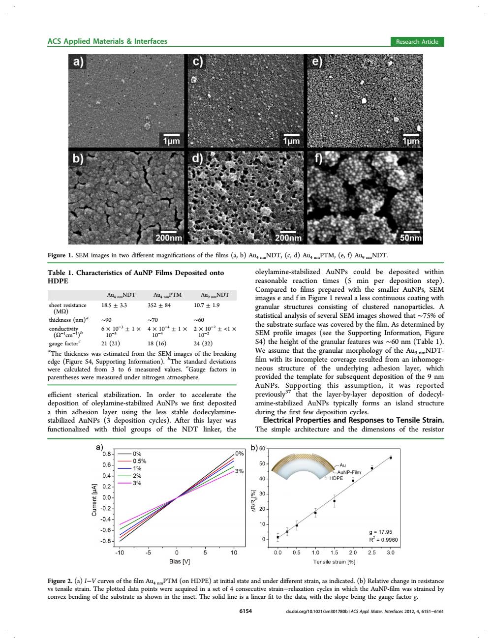
ACS Applied Materials Interfaces Research Article a um um 200nm 200nm 50nm Figure 1.SEM images in two different magnifications of the films (a,b)AuNDT,(c,d)AumPTM,(e,f)AuNDT. Table 1.Characteristics of AuNP Films Deposited onto oleylamine-stabilized AuNPs could be deposited within HDPE reasonable reaction times (5 min per deposition step). Aus NDT AuPTM Auy aNDT Compared to films prepared with the smaller AuNPs,SEM images e and f in Figure 1 reveal a less continuous coating with sheet resistance 18.5±33 352±84 10.7±1.9 (MQ2) granular structures consisting of clustered nanoparticles.A thickness(nm)4 statistical analysis of several SEM images showed that ~75%of 90 70 60 the substrate surface was covered by the film.As determined by conductivity (Q-cm-i) 6X1×400±1209±1× 10N SEM profile images (see the Supporting Information,Figure gauge factor 21(21) 18(16) 24(32) S4)the height of the granular features was ~60 nm(Table 1). "The thickness was estimated from the SEM images of the breaking We assume that the granular morphology of the AugmNDT- edge (Figure S4,Supporting Information).The standard deviations film with its incomplete coverage resulted from an inhomoge- were calculated from 3 to 6 measured values.Gauge factors in neous structure of the underlying adhesion layer,which parentheses were measured under nitrogen atmosphere. provided the template for subsequent deposition of the 9 nm AuNPs.Supporting this assumption,it was reported efficient sterical stabilization.In order to accelerate the previously37 that the layer-by-layer deposition of dodecyl- deposition of oleylamine-stabilized AuNPs we first deposited amine-stabilized AuNPs typically forms an island structure a thin adhesion layer using the less stable dodecylamine- during the first few deposition cycles. stabilized AuNPs (3 deposition cycles).After this layer was Electrical Properties and Responses to Tensile Strain. functionalized with thiol groups of the NDT linker,the The simple architecture and the dimensions of the resistor a) b)60 0.8- 0% 0% 0.6- 0.5% 1% Au % 2% AuNP-Film HDPE 02 3% 0. 30- -0.2 20 10- -0.6 9=17.95 -0.8 R2=0.9960 -10 0 10 0.0 0.5 1.01.5 2.0 25 3.0 Bias [V] Tensile strain [% Figure 2.(a)I-V curves of the film AuPTM (on HDPE)at initial state and under different strain,as indicated.(b)Relative change in resistance vs tensile strain.The plotted data points were acquired in a set of 4 consecutive strain-relaxation cycles in which the AuNP-film was strained by convex bending of the substrate as shown in the inset.The solid line is a linear fit to the data,with the slope being the gauge factor g. 6154 dx.doLorg/10.1021/am301780bl ACS Appl.Mater.Interfaces 2012,4,6151-6161efficient sterical stabilization. In order to accelerate the deposition of oleylamine-stabilized AuNPs we first deposited a thin adhesion layer using the less stable dodecylaminestabilized AuNPs (3 deposition cycles). After this layer was functionalized with thiol groups of the NDT linker, the oleylamine-stabilized AuNPs could be deposited within reasonable reaction times (5 min per deposition step). Compared to films prepared with the smaller AuNPs, SEM images e and f in Figure 1 reveal a less continuous coating with granular structures consisting of clustered nanoparticles. A statistical analysis of several SEM images showed that ∼75% of the substrate surface was covered by the film. As determined by SEM profile images (see the Supporting Information, Figure S4) the height of the granular features was ∼60 nm (Table 1). We assume that the granular morphology of the Au9 nmNDT- film with its incomplete coverage resulted from an inhomogeneous structure of the underlying adhesion layer, which provided the template for subsequent deposition of the 9 nm AuNPs. Supporting this assumption, it was reported previously37 that the layer-by-layer deposition of dodecylamine-stabilized AuNPs typically forms an island structure during the first few deposition cycles. Electrical Properties and Responses to Tensile Strain. The simple architecture and the dimensions of the resistor Figure 1. SEM images in two different magnifications of the films (a, b) Au4 nmNDT, (c, d) Au4 nmPTM, (e, f) Au9 nmNDT. Table 1. Characteristics of AuNP Films Deposited onto HDPE Au4 nmNDT Au4 nmPTM Au9 nmNDT sheet resistance (MΩ) 18.5 ± 3.3 352 ± 84 10.7 ± 1.9 thickness (nm)a ∼90 ∼70 ∼60 conductivity (Ω−1 cm−1 ) b 6 × 10⁻³ ± 1 × 10⁻³ 4 × 10⁻⁴ ± 1 × 10⁻⁴ 2 × 10⁻² ± <1 × 10⁻² gauge factorc 21 (21) 18 (16) 24 (32) a The thickness was estimated from the SEM images of the breaking edge (Figure S4, Supporting Information). b The standard deviations were calculated from 3 to 6 measured values. c Gauge factors in parentheses were measured under nitrogen atmosphere. Figure 2. (a) I−V curves of the film Au4 nmPTM (on HDPE) at initial state and under different strain, as indicated. (b) Relative change in resistance vs tensile strain. The plotted data points were acquired in a set of 4 consecutive strain−relaxation cycles in which the AuNP-film was strained by convex bending of the substrate as shown in the inset. The solid line is a linear fit to the data, with the slope being the gauge factor g. ACS Applied Materials & Interfaces Research Article 6154 dx.doi.org/10.1021/am301780b | ACS Appl. Mater. Interfaces 2012, 4, 6151−6161