正在加载图片...
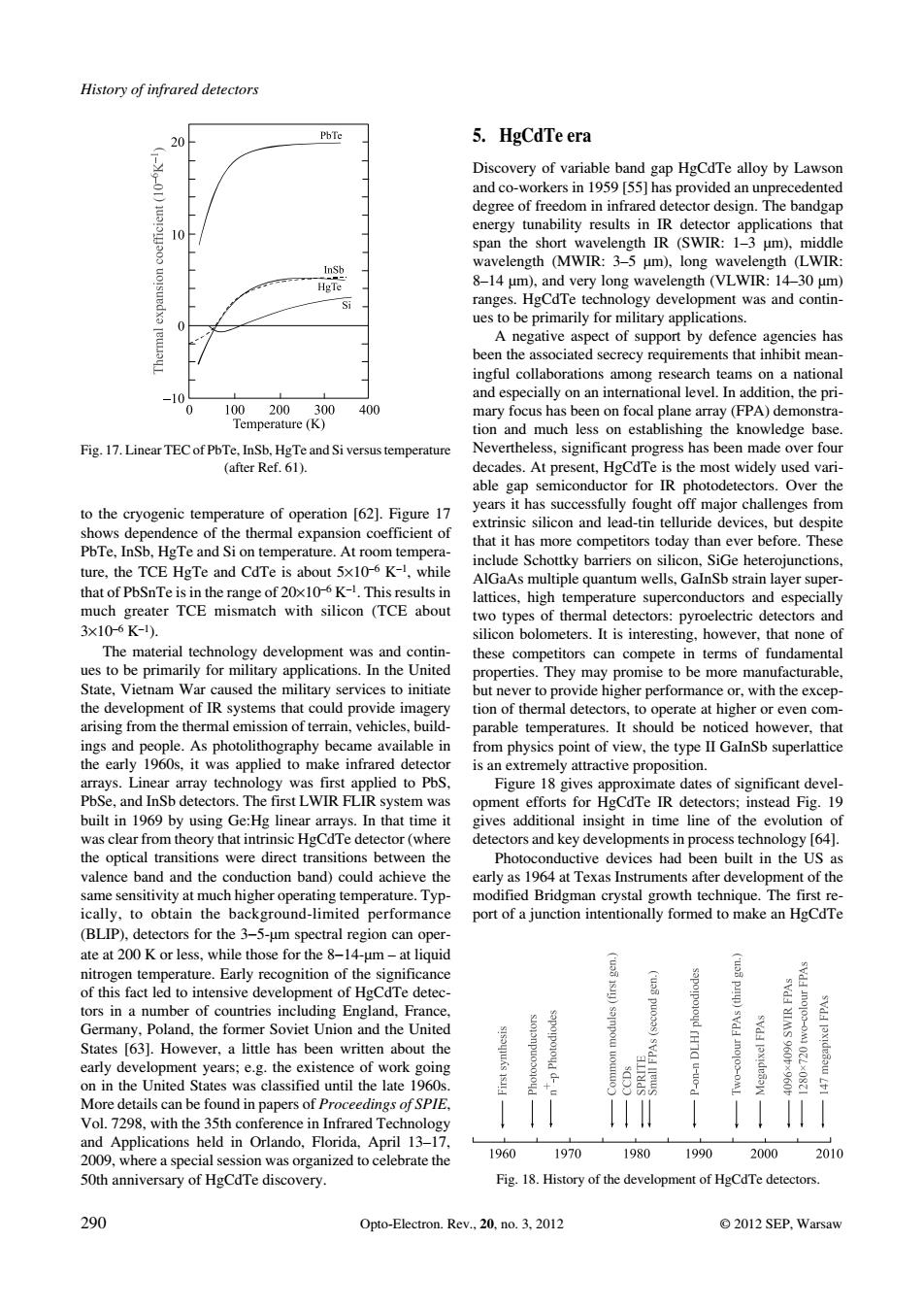
History of infrared detectors 20 5.HgCdTeera Discovery of variable band gap HgCdTe alloy by Lawso span the shor ogy deve eth (VLWIR:14-30 um opment was and contin ues to be primarly or cies ha been the associated that inhibit mean 00 400 est Fig.17.Linea and ing the knowledge ades.At pres HgCdTe is the most widely used var gap s for IR phote dete to the c enic tem e17 silicon and lead-tin teluride devices,but de today tha AlGaAs multiple quantum wells.GalnSb strain laver sup w10-6w-1T much greater TCE mismatch with silicon (TCE about 3x10-K- eters It is interesting however that none o hese itors can compet terms of fundam State.Vietam War aused the military services to initiate with the e could prov ings and people.As photolithog nhy became availahle in the ty the early 1960s,it wa applied to make nfrared de is an on 1g0 built n1by using Ge:arays.In that time additional insight in time line of the ev detector (wn valence band and the 1dcoud Texas In evel nt of th to obt ally fo (BI IP)detectors for the 3-5-um spectral region ca ate at 200 K or less.while those for the 8-14-um-at liquid recognition of th tors in a number of countries including Eng and.Fr and,the forn Un 63 early e g the existence classified until the late Vol.7298.with the 35thc and ate th 1960 1970 1980 1990 2000 2010 50h wnere a sp yof HgCdTe dis Fig.18.History of the deve nt of HecdTe detectors 290 Opto-Electron.Rev.20.no.3.2012 2012 SEP.Warsawto the cryogenic temperature of operation [62]. Figure 17 shows dependence of the thermal expansion coefficient of PbTe, InSb, HgTe and Si on temperature. At room tempera− ture, the TCE HgTe and CdTe is about 5
10–6 K–1, while that of PbSnTe is in the range of 20
10–6 K–1. This results in much greater TCE mismatch with silicon (TCE about 3
10–6 K–1). The material technology development was and contin− ues to be primarily for military applications. In the United State, Vietnam War caused the military services to initiate the development of IR systems that could provide imagery arising from the thermal emission of terrain, vehicles, build− ings and people. As photolithography became available in the early 1960s, it was applied to make infrared detector arrays. Linear array technology was first applied to PbS, PbSe, and InSb detectors. The first LWIR FLIR system was built in 1969 by using Ge:Hg linear arrays. In that time it was clear from theory that intrinsic HgCdTe detector (where the optical transitions were direct transitions between the valence band and the conduction band) could achieve the same sensitivity at much higher operating temperature. Typ− ically, to obtain the background−limited performance (BLIP), detectors for the 3
5−μm spectral region can oper− ate at 200 K or less, while those for the 8
14−μm – at liquid nitrogen temperature. Early recognition of the significance of this fact led to intensive development of HgCdTe detec− tors in a number of countries including England, France, Germany, Poland, the former Soviet Union and the United States [63]. However, a little has been written about the early development years; e.g. the existence of work going on in the United States was classified until the late 1960s. More details can be found in papers of Proceedings of SPIE, Vol. 7298, with the 35th conference in Infrared Technology and Applications held in Orlando, Florida, April 13–17, 2009, where a special session was organized to celebrate the 50th anniversary of HgCdTe discovery. 5. HgCdTe era Discovery of variable band gap HgCdTe alloy by Lawson and co−workers in 1959 [55] has provided an unprecedented degree of freedom in infrared detector design. The bandgap energy tunability results in IR detector applications that span the short wavelength IR (SWIR: 1–3 μm), middle wavelength (MWIR: 3–5 μm), long wavelength (LWIR: 8–14 μm), and very long wavelength (VLWIR: 14–30 μm) ranges. HgCdTe technology development was and contin− ues to be primarily for military applications. A negative aspect of support by defence agencies has been the associated secrecy requirements that inhibit mean− ingful collaborations among research teams on a national and especially on an international level. In addition, the pri− mary focus has been on focal plane array (FPA) demonstra− tion and much less on establishing the knowledge base. Nevertheless, significant progress has been made over four decades. At present, HgCdTe is the most widely used vari− able gap semiconductor for IR photodetectors. Over the years it has successfully fought off major challenges from extrinsic silicon and lead−tin telluride devices, but despite that it has more competitors today than ever before. These include Schottky barriers on silicon, SiGe heterojunctions, AlGaAs multiple quantum wells, GaInSb strain layer super− lattices, high temperature superconductors and especially two types of thermal detectors: pyroelectric detectors and silicon bolometers. It is interesting, however, that none of these competitors can compete in terms of fundamental properties. They may promise to be more manufacturable, but never to provide higher performance or, with the excep− tion of thermal detectors, to operate at higher or even com− parable temperatures. It should be noticed however, that from physics point of view, the type II GaInSb superlattice is an extremely attractive proposition. Figure 18 gives approximate dates of significant devel− opment efforts for HgCdTe IR detectors; instead Fig. 19 gives additional insight in time line of the evolution of detectors and key developments in process technology [64]. Photoconductive devices had been built in the US as early as 1964 at Texas Instruments after development of the modified Bridgman crystal growth technique. The first re− port of a junction intentionally formed to make an HgCdTe History of infrared detectors 290 Opto−Electron. Rev., 20, no. 3, 2012 © 2012 SEP, Warsaw Fig. 17. Linear TEC of PbTe, InSb, HgTe and Si versus temperature (after Ref. 61). Fig. 18. History of the development of HgCdTe detectors