正在加载图片...
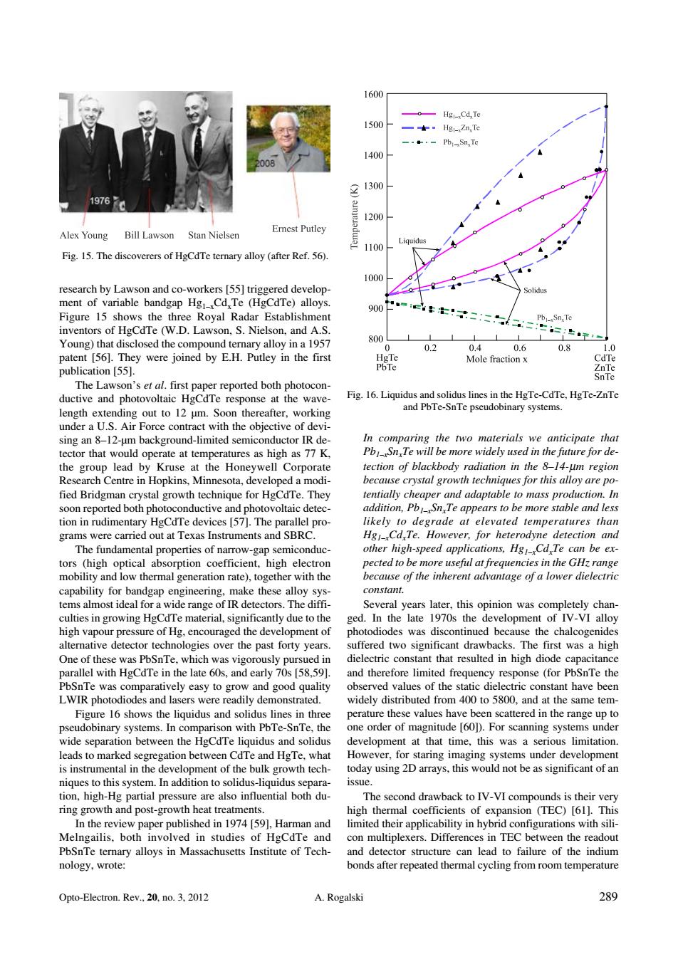
<00 .th.Sn.te 400 19767e Alex Young Bill Lawson Stan Nielsen Emest Putley 110 Fig.15.The discoverers of HCTe alloy(after Ref.56) 1000 ch by la ment of variable bandgap HgCd.Te (HgCdTe)alloys You g)that closed the co und tern ry alloy in a 1957 0.2 0.8 The lawson's et al.first of de sing an 8-12-um background-limited semico nductor IR de ection of blackbody radiat n in the 8-14-um region a mod ble and les tion in rudime lel pro elevated temperatures tha ruments tors(high optical high electron m lity and thermal generat n rate).togeth ith the ed.In the late 1s the development t of IV-VI altemative detector technologies over the past forty vears ctrc constant that resulted in high diod .10 LWIR pho widely distributed from 400 to 5800.and at the same tem and sor quidus levelopment at that time,this was a serious limitation d o marked se dTe high-Hg partial pr o-VIcom paper published in 1974 (591.Harman and involve studies of HgCdTe and ween the re setts Institute of Tech Opto-Electron.Rev.20.n.3.2012 A.Rogalski 289 research by Lawson and co−workers [55] triggered develop− ment of variable bandgap Hg1–xCdxTe (HgCdTe) alloys. Figure 15 shows the three Royal Radar Establishment inventors of HgCdTe (W.D. Lawson, S. Nielson, and A.S. Young) that disclosed the compound ternary alloy in a 1957 patent [56]. They were joined by E.H. Putley in the first publication [55]. The Lawson’s et al. first paper reported both photocon− ductive and photovoltaic HgCdTe response at the wave− length extending out to 12 μm. Soon thereafter, working under a U.S. Air Force contract with the objective of devi− sing an 8–12−μm background−limited semiconductor IR de− tector that would operate at temperatures as high as 77 K, the group lead by Kruse at the Honeywell Corporate Research Centre in Hopkins, Minnesota, developed a modi− fied Bridgman crystal growth technique for HgCdTe. They soon reported both photoconductive and photovoltaic detec− tion in rudimentary HgCdTe devices [57]. The parallel pro− grams were carried out at Texas Instruments and SBRC. The fundamental properties of narrow−gap semiconduc− tors (high optical absorption coefficient, high electron mobility and low thermal generation rate), together with the capability for bandgap engineering, make these alloy sys− tems almost ideal for a wide range of IR detectors. The diffi− culties in growing HgCdTe material, significantly due to the high vapour pressure of Hg, encouraged the development of alternative detector technologies over the past forty years. One of these was PbSnTe, which was vigorously pursued in parallel with HgCdTe in the late 60s, and early 70s [58,59]. PbSnTe was comparatively easy to grow and good quality LWIR photodiodes and lasers were readily demonstrated. Figure 16 shows the liquidus and solidus lines in three pseudobinary systems. In comparison with PbTe−SnTe, the wide separation between the HgCdTe liquidus and solidus leads to marked segregation between CdTe and HgTe, what is instrumental in the development of the bulk growth tech− niques to this system. In addition to solidus−liquidus separa− tion, high−Hg partial pressure are also influential both du− ring growth and post−growth heat treatments. In the review paper published in 1974 [59], Harman and Melngailis, both involved in studies of HgCdTe and PbSnTe ternary alloys in Massachusetts Institute of Tech− nology, wrote: In comparing the two materials we anticipate that Pb1–xSnxTe will be more widely used in the future for de− tection of blackbody radiation in the 8–14−m region because crystal growth techniques for this alloy are po− tentially cheaper and adaptable to mass production. In addition, Pb1–xSnxTe appears to be more stable and less likely to degrade at elevated temperatures than Hg1–xCdxTe. However, for heterodyne detection and other high−speed applications, Hg1–xCdxTe can be ex− pected to be more useful at frequencies in the GHz range because of the inherent advantage of a lower dielectric constant. Several years later, this opinion was completely chan− ged. In the late 1970s the development of IV−VI alloy photodiodes was discontinued because the chalcogenides suffered two significant drawbacks. The first was a high dielectric constant that resulted in high diode capacitance and therefore limited frequency response (for PbSnTe the observed values of the static dielectric constant have been widely distributed from 400 to 5800, and at the same tem− perature these values have been scattered in the range up to one order of magnitude [60]). For scanning systems under development at that time, this was a serious limitation. However, for staring imaging systems under development today using 2D arrays, this would not be as significant of an issue. The second drawback to IV−VI compounds is their very high thermal coefficients of expansion (TEC) [61]. This limited their applicability in hybrid configurations with sili− con multiplexers. Differences in TEC between the readout and detector structure can lead to failure of the indium bonds after repeated thermal cycling from room temperature Opto−Electron. Rev., 20, no. 3, 2012 A. Rogalski 289 Fig. 15. The discoverers of HgCdTe ternary alloy (after Ref. 56). Fig. 16. Liquidus and solidus lines in the HgTe−CdTe, HgTe−ZnTe and PbTe−SnTe pseudobinary systems