正在加载图片...
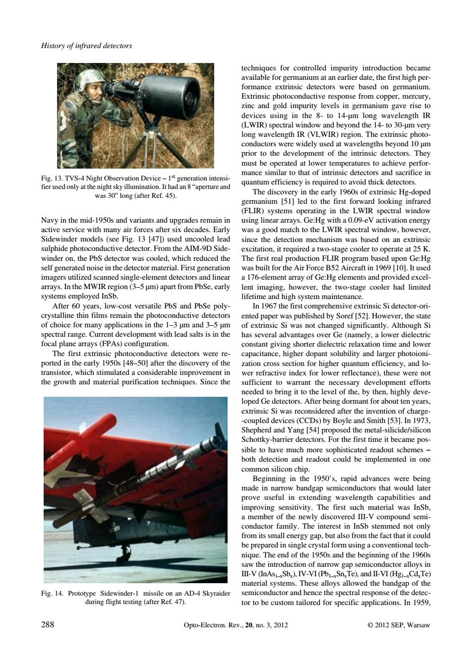
History of infrared detectors techniques for controled impurity introduction became cuc opet ercary. m is required to avoidthick detectors sing lin oled lead cction mechanism was based on sulphide photoconductive detector From the AIM-9D Side age cooler to operate at 25 however.the two-stage After60 years.low-cost versatile PbS and PbSe poly ctor-on d3-5 d by Soref 52 the state nd lowe ration cro section for hisher quantum eff and lo ance). hes eeded to bring it to the level of the by then,highly deve oped Ge ctors.After being dormant for abou n year on chip. nade in nan ful in extend wavelength capabilitie cor family. nique.The end of the 1950s and the beginning of the 1960 SIV-VIPSn.Te) naterial systems.These alloys allowed the bandgap of th 288 Opto-Electron.Rev.20.no.3.2012 2012 SEP.WarsawNavy in the mid−1950s and variants and upgrades remain in active service with many air forces after six decades. Early Sidewinder models (see Fig. 13 [47]) used uncooled lead sulphide photoconductive detector. From the AIM−9D Side− winder on, the PbS detector was cooled, which reduced the self generated noise in the detector material. First generation imagers utilized scanned single−element detectors and linear arrays. In the MWIR region (3–5 μm) apart from PbSe, early systems employed InSb. After 60 years, low−cost versatile PbS and PbSe poly− crystalline thin films remain the photoconductive detectors of choice for many applications in the 1–3 μm and 3–5 μm spectral range. Current development with lead salts is in the focal plane arrays (FPAs) configuration. The first extrinsic photoconductive detectors were re− ported in the early 1950s [48–50] after the discovery of the transistor, which stimulated a considerable improvement in the growth and material purification techniques. Since the techniques for controlled impurity introduction became available for germanium at an earlier date, the first high per− formance extrinsic detectors were based on germanium. Extrinsic photoconductive response from copper, mercury, zinc and gold impurity levels in germanium gave rise to devices using in the 8− to 14−μm long wavelength IR (LWIR) spectral window and beyond the 14− to 30−μm very long wavelength IR (VLWIR) region. The extrinsic photo− conductors were widely used at wavelengths beyond 10 μm prior to the development of the intrinsic detectors. They must be operated at lower temperatures to achieve perfor− mance similar to that of intrinsic detectors and sacrifice in quantum efficiency is required to avoid thick detectors. The discovery in the early 1960s of extrinsic Hg−doped germanium [51] led to the first forward looking infrared (FLIR) systems operating in the LWIR spectral window using linear arrays. Ge:Hg with a 0.09−eV activation energy was a good match to the LWIR spectral window, however, since the detection mechanism was based on an extrinsic excitation, it required a two−stage cooler to operate at 25 K. The first real production FLIR program based upon Ge:Hg was built for the Air Force B52 Aircraft in 1969 [10]. It used a 176−element array of Ge:Hg elements and provided excel− lent imaging, however, the two−stage cooler had limited lifetime and high system maintenance. In 1967 the first comprehensive extrinsic Si detector−ori− ented paper was published by Soref [52]. However, the state of extrinsic Si was not changed significantly. Although Si has several advantages over Ge (namely, a lower dielectric constant giving shorter dielectric relaxation time and lower capacitance, higher dopant solubility and larger photoioni− zation cross section for higher quantum efficiency, and lo− wer refractive index for lower reflectance), these were not sufficient to warrant the necessary development efforts needed to bring it to the level of the, by then, highly deve− loped Ge detectors. After being dormant for about ten years, extrinsic Si was reconsidered after the invention of charge− −coupled devices (CCDs) by Boyle and Smith [53]. In 1973, Shepherd and Yang [54] proposed the metal−silicide/silicon Schottky−barrier detectors. For the first time it became pos− sible to have much more sophisticated readout schemes
both detection and readout could be implemented in one common silicon chip. Beginning in the 1950’s, rapid advances were being made in narrow bandgap semiconductors that would later prove useful in extending wavelength capabilities and improving sensitivity. The first such material was InSb, a member of the newly discovered III−V compound semi− conductor family. The interest in InSb stemmed not only from its small energy gap, but also from the fact that it could be prepared in single crystal form using a conventional tech− nique. The end of the 1950s and the beginning of the 1960s saw the introduction of narrow gap semiconductor alloys in III−V (InAs1–xSbx), IV−VI (Pb1–xSnxTe), and II−VI (Hg1–xCdxTe) material systems. These alloys allowed the bandgap of the semiconductor and hence the spectral response of the detec− tor to be custom tailored for specific applications. In 1959, History of infrared detectors 288 Opto−Electron. Rev., 20, no. 3, 2012 © 2012 SEP, Warsaw Fig. 13. TVS−4 Night Observation Device – 1st generation intensi− fier used only at the night sky illumination. It had an 8 “aperture and was 30” long (after Ref. 45). Fig. 14. Prototype Sidewinder−1 missile on an AD−4 Skyraider during flight testing (after Ref. 47)