正在加载图片...
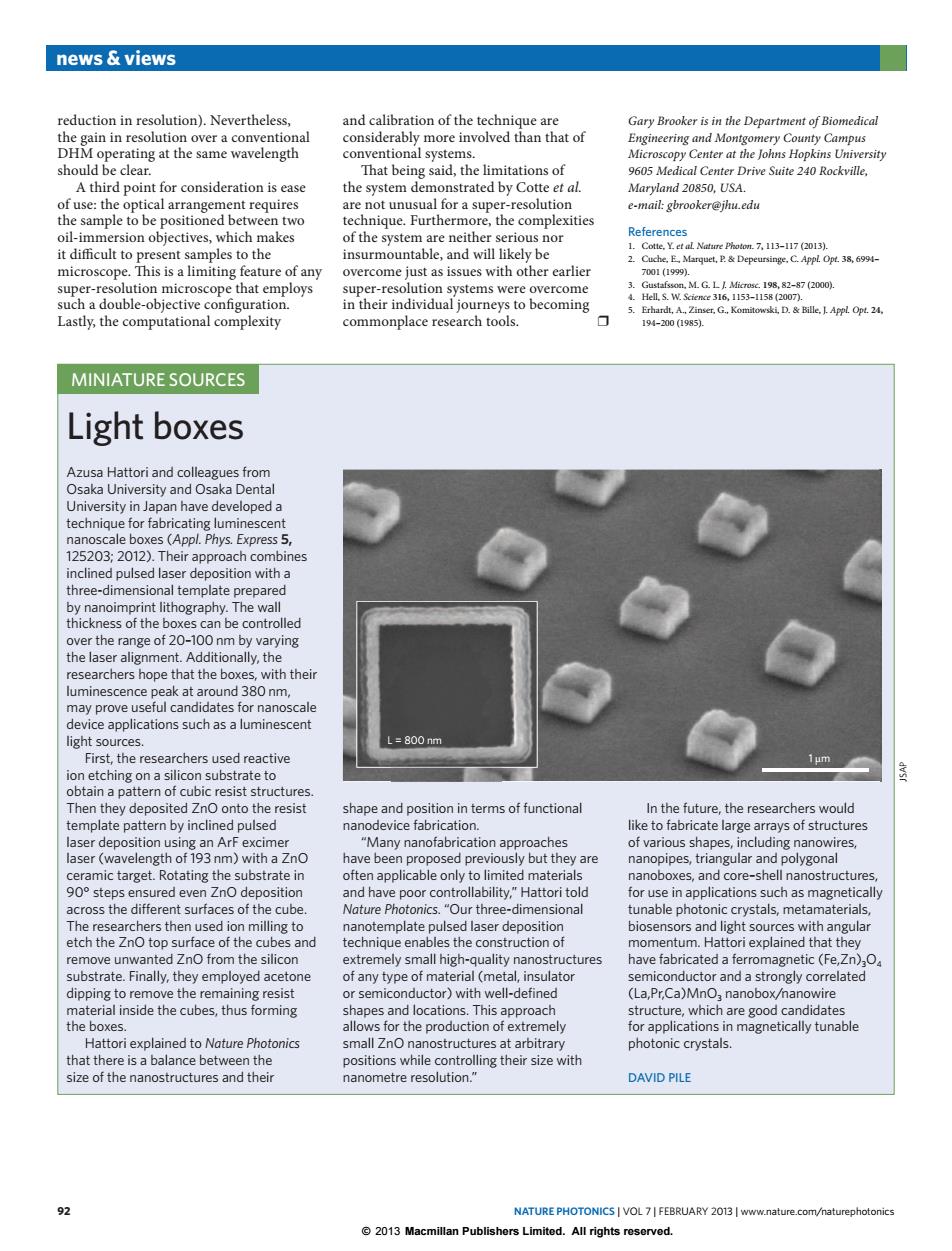
news views reduction in resolution).Nevertheless, and calibration of the technique are Gary Brooker is in the Department of Biomedical the gain in resolution over a conventional considerably more involved than that of Engineering and Montgomery County Campus DHM operating at the same wavelength conventional systems Microscopy Center at the Johns Hopkins University should be clear. That being said,the limitations of 9605 Medical Center Drive Suite 240 Rockville, A third point for consideration is ease the system demonstrated by Cotte et al. Maryland 20850,USA. of use:the optical arrangement requires are not unusual for a super-resolution e-mail:gbrooker@jhu.edu the sample to be positioned between two technique.Furthermore,the complexities oil-immersion objectives,which makes of the system are neither serious nor References 1.Cotte,Y.et al.Nature Photon.7,113-117 (2013). it difficult to present samples to the insurmountable,and will likely be 2.Cuche.E.Marquet P&Depeursinge.C.Appl Opt.386994- microscope.This is a limiting feature of any overcome just as issues with other earlier 7001(1999). super-resolution microscope that employs super-resolution systems were overcome 3.Gustafsson.M.G.L.Microsc.198,82-87(2000) such a double-objective configuration. in their individual journeys to becoming 4.Hel.S.W.Science316,1153-l158(2007). 5.Erhardt,A..Zinser,G..Komitowski,D.Bille,J.Appl.Opt.24. Lastly,the computational complexity commonplace research tools. 194-200(1985). MINIATURE SOURCES Light boxes Azusa Hattori and colleagues from Osaka University and Osaka Dental University in Japan have developed a technique for fabricating luminescent nanoscale boxes (Appl.Phys.Express 5 125203;2012).Their approach combines inclined pulsed laser deposition with a three-dimensional template prepared by nanoimprint lithography.The wall thickness of the boxes can be controlled over the range of 20-100 nm by varying the laser alignment.Additionally,the researchers hope that the boxes,with their uminescence peak at around 380 nm, may prove useful candidates for nanoscale device applications such as a luminescent light sources. L=800 nm First,the researchers used reactive m ion etching on a silicon substrate to obtain a pattern of cubic resist structures. Then they deposited ZnO onto the resist shape and position in terms of functional In the future.the researchers would template pattern by inclined pulsed nanodevice fabrication. like to fabricate large arrays of structures laser deposition using an ArF excimer "Many nanofabrication approaches of various shapes,including nanowires, laser (wavelength of 193 nm)with a ZnO have been proposed previously but they are nanopipes,triangular and polygonal ceramic target.Rotating the substrate in often applicable only to limited materials nanoboxes,and core-shell nanostructures, 90 steps ensured even ZnO deposition and have poor controllability,"Hattori told for use in applications such as magnetically across the different surfaces of the cube Nature Photonics."Our three-dimensional tunable photonic crystals,metamaterials, The researchers then used ion milling to nanotemplate pulsed laser deposition biosensors and light sources with angular etch the ZnO top surface of the cubes and technique enables the construction of momentum.Hattori explained that they remove unwanted ZnO from the silicon extremely small high-quality nanostructures have fabricated a ferromagnetic (Fe,Zn).O substrate.Finally,they employed acetone of any type of material (metal,insulator semiconductor and a strongly correlated dipping to remove the remaining resist or semiconductor)with well-defined (La,Pr,Ca)MnO,nanobox/nanowire material inside the cubes,thus forming shapes and locations.This approach structure,which are good candidates the boxes. allows for the production of extremely for applications in magnetically tunable Hattori explained to Nature Photonics small ZnO nanostructures at arbitrary photonic crystals. that there is a balance between the positions while controlling their size with size of the nanostructures and their nanometre resolution." DAVID PILE g NATURE PHOTONICS VOL 7|FEBRUARY 2013 www.nature.com/naturephotonics 2013 Macmillan Publishers Limited.All rights reserved.© 2013 Macmillan Publishers Limited. All rights reserved. 92 NATURE PHOTONICS | VOL 7 | FEBRUARY 2013 | www.nature.com/naturephotonics news & views reduction in resolution). Nevertheless, the gain in resolution over a conventional DHM operating at the same wavelength should be clear. A third point for consideration is ease of use: the optical arrangement requires the sample to be positioned between two oil-immersion objectives, which makes it difficult to present samples to the microscope. This is a limiting feature of any super-resolution microscope that employs such a double-objective configuration. Lastly, the computational complexity and calibration of the technique are considerably more involved than that of conventional systems. That being said, the limitations of the system demonstrated by Cotte et al. are not unusual for a super-resolution technique. Furthermore, the complexities of the system are neither serious nor insurmountable, and will likely be overcome just as issues with other earlier super-resolution systems were overcome in their individual journeys to becoming commonplace research tools. ❒ Gary Brooker is in the Department of Biomedical Engineering and Montgomery County Campus Microscopy Center at the Johns Hopkins University 9605 Medical Center Drive Suite 240 Rockville, Maryland 20850, USA. e-mail: gbrooker@jhu.edu References 1. Cotte, Y. et al. Nature Photon. 7, 113–117 (2013). 2. Cuche, E., Marquet, P. & Depeursinge, C. Appl. Opt. 38, 6994– 7001 (1999). 3. Gustafsson, M. G. L. J. Microsc. 198, 82–87 (2000). 4. Hell, S. W. Science 316, 1153–1158 (2007). 5. Erhardt, A., Zinser, G., Komitowski, D. & Bille, J. Appl. Opt. 24, 194–200 (1985). 1 μm L = 800 nm Azusa Hattori and colleagues from Osaka University and Osaka Dental University in Japan have developed a technique for fabricating luminescent nanoscale boxes (Appl. Phys. Express 5, 125203; 2012). Their approach combines inclined pulsed laser deposition with a three-dimensional template prepared by nanoimprint lithography. The wall thickness of the boxes can be controlled over the range of 20–100 nm by varying the laser alignment. Additionally, the researchers hope that the boxes, with their luminescence peak at around 380 nm, may prove useful candidates for nanoscale device applications such as a luminescent light sources. First, the researchers used reactive ion etching on a silicon substrate to obtain a pattern of cubic resist structures. Then they deposited ZnO onto the resist template pattern by inclined pulsed laser deposition using an ArF excimer laser (wavelength of 193 nm) with a ZnO ceramic target. Rotating the substrate in 90° steps ensured even ZnO deposition across the different surfaces of the cube. The researchers then used ion milling to etch the ZnO top surface of the cubes and remove unwanted ZnO from the silicon substrate. Finally, they employed acetone dipping to remove the remaining resist material inside the cubes, thus forming the boxes. Hattori explained to Nature Photonics that there is a balance between the size of the nanostructures and their Light boxes MINIATURE SOURCES shape and position in terms of functional nanodevice fabrication. “Many nanofabrication approaches have been proposed previously but they are often applicable only to limited materials and have poor controllability,” Hattori told Nature Photonics. “Our three-dimensional nanotemplate pulsed laser deposition technique enables the construction of extremely small high-quality nanostructures of any type of material (metal, insulator or semiconductor) with well-defined shapes and locations. This approach allows for the production of extremely small ZnO nanostructures at arbitrary positions while controlling their size with nanometre resolution.” In the future, the researchers would like to fabricate large arrays of structures of various shapes, including nanowires, nanopipes, triangular and polygonal nanoboxes, and core–shell nanostructures, for use in applications such as magnetically tunable photonic crystals, metamaterials, biosensors and light sources with angular momentum. Hattori explained that they have fabricated a ferromagnetic (Fe,Zn)3O4 semiconductor and a strongly correlated (La,Pr,Ca)MnO3 nanobox/nanowire structure, which are good candidates for applications in magnetically tunable photonic crystals. DAVID PILE 1 μm L = 800 nm JSAP