正在加载图片...
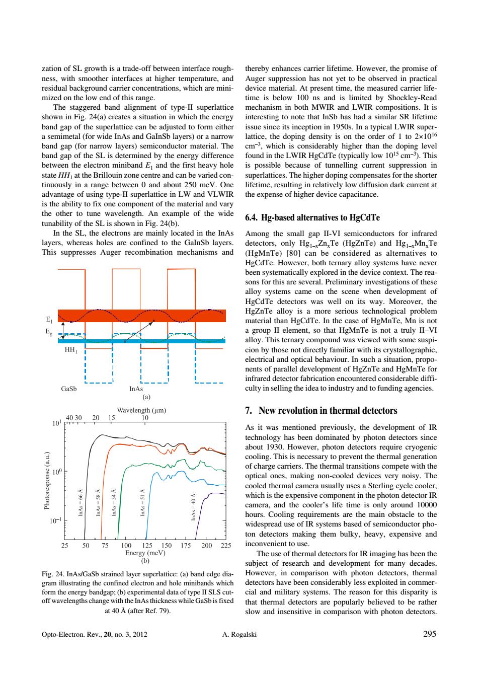
zation of SLgrowth is a trade-off between interface rough thereby enhances lifetime.However,the promise this range ime d by Shockley-Rea shown in E可i24 a)cre nteresting to note that InSp has had a similar SR lifetime band gap of the superlattice can be adjusted to form eithe .natypical LWIR band gap(fo (or wic band gap of the SL is ned by the enery difference found in the LWIR HgCdTe (typically at the Bri hol high tinuously in a range betweenand about ifetime.resu shorte in relatively lowdiffusion dark current the expen of higher device capacitance. tuna SL is showr in Fig. 6.4.Hg-based alternatives to HgCdTe d in the InA .e () ctors for infr can be consic ed as altem natives to acayeporh The of thes on its ZnTe lloy is a more se rious techn ogical 1g This temary compound was viewed with ment of heznte and Hemnte a 7.New revolution in thermal detectors 10140302015 As it was mentioned previously.the development of IR technology has been dominated by photon detectors sinc of charge carriers.The ther ransitions compe with th nes,m king non-c era. the cooler's sonly aroun 0 ctors making them bulky,heavy,expensive and 175 200 225 The use of thermal detectors for IR imaging has been the ubject of esearch and de elop ment for many dec cial and military systems.The reason for this at 40 A (after Ref.79) Opto-Electron.Rev.20.no 3 2012 295 zation of SL growth is a trade−off between interface rough− ness, with smoother interfaces at higher temperature, and residual background carrier concentrations, which are mini− mized on the low end of this range. The staggered band alignment of type−II superlattice shown in Fig. 24(a) creates a situation in which the energy band gap of the superlattice can be adjusted to form either a semimetal (for wide InAs and GaInSb layers) or a narrow band gap (for narrow layers) semiconductor material. The band gap of the SL is determined by the energy difference between the electron miniband E1 and the first heavy hole state HH1 at the Brillouin zone centre and can be varied con− tinuously in a range between 0 and about 250 meV. One advantage of using type−II superlattice in LW and VLWIR is the ability to fix one component of the material and vary the other to tune wavelength. An example of the wide tunability of the SL is shown in Fig. 24(b). In the SL, the electrons are mainly located in the InAs layers, whereas holes are confined to the GaInSb layers. This suppresses Auger recombination mechanisms and thereby enhances carrier lifetime. However, the promise of Auger suppression has not yet to be observed in practical device material. At present time, the measured carrier life− time is below 100 ns and is limited by Shockley−Read mechanism in both MWIR and LWIR compositions. It is interesting to note that InSb has had a similar SR lifetime issue since its inception in 1950s. In a typical LWIR super− lattice, the doping density is on the order of 1 to 2×1016 cm–3, which is considerably higher than the doping level found in the LWIR HgCdTe (typically low 1015 cm–3). This is possible because of tunnelling current suppression in superlattices. The higher doping compensates for the shorter lifetime, resulting in relatively low diffusion dark current at the expense of higher device capacitance. 6.4. Hg-based alternatives to HgCdTe Among the small gap II−VI semiconductors for infrared detectors, only Hg1–xZnxTe (HgZnTe) and Hg1–xMnxTe (HgMnTe) [80] can be considered as alternatives to HgCdTe. However, both ternary alloy systems have never been systematically explored in the device context. The rea− sons for this are several. Preliminary investigations of these alloy systems came on the scene when development of HgCdTe detectors was well on its way. Moreover, the HgZnTe alloy is a more serious technological problem material than HgCdTe. In the case of HgMnTe, Mn is not a group II element, so that HgMnTe is not a truly II–VI alloy. This ternary compound was viewed with some suspi− cion by those not directly familiar with its crystallographic, electrical and optical behaviour. In such a situation, propo− nents of parallel development of HgZnTe and HgMnTe for infrared detector fabrication encountered considerable diffi− culty in selling the idea to industry and to funding agencies. 7. New revolution in thermal detectors As it was mentioned previously, the development of IR technology has been dominated by photon detectors since about 1930. However, photon detectors require cryogenic cooling. This is necessary to prevent the thermal generation of charge carriers. The thermal transitions compete with the optical ones, making non−cooled devices very noisy. The cooled thermal camera usually uses a Sterling cycle cooler, which is the expensive component in the photon detector IR camera, and the cooler’s life time is only around 10000 hours. Cooling requirements are the main obstacle to the widespread use of IR systems based of semiconductor pho− ton detectors making them bulky, heavy, expensive and inconvenient to use. The use of thermal detectors for IR imaging has been the subject of research and development for many decades. However, in comparison with photon detectors, thermal detectors have been considerably less exploited in commer− cial and military systems. The reason for this disparity is that thermal detectors are popularly believed to be rather slow and insensitive in comparison with photon detectors. Opto−Electron. Rev., 20, no. 3, 2012 A. Rogalski 295 Fig. 24. InAs/GaSb strained layer superlattice: (a) band edge dia− gram illustrating the confined electron and hole minibands which form the energy bandgap; (b) experimental data of type II SLS cut− off wavelengths change with the InAs thickness while GaSb is fixed at 40 (after Ref. 79).�