正在加载图片...
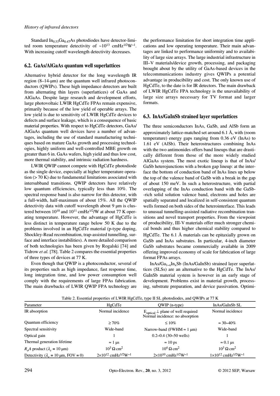
History of infrared detectors the performance limitation for short integration time appli 6.2.GaAs/AIGaAs quantum well superlattices of GaAs.h telecommunications industry gives QWIPs a potentia um)are the tum well infrared phot of Gae buil of LWIR HgCdTe FPA technology is the unavailability of ch and development efforts large pho olta As ren ommafor Tmacr 6.3.InAs/GaInSb strained layer superlattices and surface I Heaeoeaucnc AlGaAs quantum well devices have a number of advan The thre and AISb form a rd manufacturing t ure ranging from 0.36 ev (InAs)to Their het res com ining InA low cost studied LWIR OWIP E as the single device,especially at higher tempe ature ope face the botom of cnuction band of As lines up belo tion(>70 K)due to tation tynically less than 10%The spe tral resp arrow for this ctivity data with cutoff of ngth abou on This tered between101 7K oper o unusual tunnelling-assisted radiative on trar ag From the problems involved in an HeCdTe material (p-type doping. mpared to Shockley-Red nnelling.sur HgCdTe.The 6.1 A materials can be epitaxially grown o In par ar has heen given by rogalski 171 an n200 Tidrow et al.[781.Table 2 res the essential properties offering improved economy of scale for fabrication of large of ee types /GalnSb)strained lay its ties such as high im dance fast response time tices (SLSs)aren to the Hecdre.The InAs long integration time, and low powe tion wel Table 2.Es ential properties of LWIR HgCdTe.type II SLphotodiodes.and QWIPsat 77K HgCd QWIP (n-type InAs/Gal b SL Normal incidence Normal incidence Quantum efficieney ≥70% ≤10% ■3040% Spectral sensitivity Wide-band nd (FWHM=1 um) Wide-band Optical gain 0.2-0.4(30-50 wells mal gen tion lifetim I us e10ps =0.15 R A product (10 um) 103cm 02em 103cm Detectivity (10 um.FOV=0 2x10¹²- 2x10¹⁰ cmHzi2W- 294 Opto-Electron.Rev.3.012 2012 SEP.WarsawStandard In0.53Ga0.47As photodiodes have detector−limi− ted room temperature detectivity of ~1013 cmHz1/2W–1. With increasing cutoff wavelength detectivity decreases. 6.2. GaAs/AlGaAs quantum well superlattices Alternative hybrid detector for the long wavelength IR region (8–14−μm) are the quantum well infrared photocon− ductors (QWIPs). These high impedance detectors are built from alternating thin layers (superlattices) of GaAs and AlGaAs. Despite large research and development efforts, large photovoltaic LWIR HgCdTe FPAs remain expensive, primarily because of the low yield of operable arrays. The low yield is due to sensitivity of LWIR HgCdTe devices to defects and surface leakage, which is a consequence of basic material properties. With respect to HgCdTe detectors, GaAs/ AlGaAs quantum well devices have a number of advan− tages, including the use of standard manufacturing techni− ques based on mature GaAs growth and processing technol− ogies, highly uniform and well−controlled MBE growth on greater than 6 in. GaAs wafers, high yield and thus low cost, more thermal stability, and intrinsic radiation hardness. LWIR QWIP cannot compete with HgCdTe photodiode as the single device, especially at higher temperature opera− tion (> 70 K) due to fundamental limitations associated with intersubband transitions. QWIP detectors have relatively low quantum efficiencies, typically less than 10%. The spectral response band is also narrow for this detector, with a full−width, half−maximum of about 15%. All the QWIP detectivity data with cutoff wavelength about 9 μm is clus− tered between 1010 and 1011 cmHz1/2/W at about 77 K oper− ating temperature. However, the advantage of HgCdTe is less distinct in temperature range below 50 K due to the problems involved in an HgCdTe material (p−type doping, Shockley−Read recombination, trap−assisted tunnelling, sur− face and interface instabilities). A more detailed comparison of both technologies has been given by Rogalski [74] and Tidrow et al. [78]. Table 2 compares the essential properties of three types of devices at 77 K. Even though that QWIP is a photoconductor, several of its properties such as high impedance, fast response time, long integration time, and low power consumption well comply with the requirements of large FPAs fabrication. The main drawbacks of LWIR QWIP FPA technology are the performance limitation for short integration time appli− cations and low operating temperature. Their main advan− tages are linked to performance uniformity and to availabi− lity of large size arrays. The large industrial infrastructure in III–V materials/device growth, processing, and packaging brought about by the utility of GaAs−based devices in the telecommunications industry gives QWIPs a potential advantage in producibility and cost. The only known use of HgCdTe, to the date is for IR detectors. The main drawback of LWIR HgCdTe FPA technology is the unavailability of large size arrays necessary for TV format and larger formats. 6.3. InAs/GaInSb strained layer superlattices The three semiconductors InAs, GaSb, and AlSb form an approximately lattice−matched set around 6.1 , with (room temperature) energy gaps ranging from 0.36 eV (InAs) to 1.61 eV (AlSb). Their heterostructures combining InAs with the two antimonides offers band lineups that are drasti− cally different from those of the more widely studied AlGaAs system. The most exotic lineup is that of InAs/ GaSb heterojunctions with a broken gap lineup: at the inter− face the bottom of conduction band of InAs lines up below the top of the valence band of GaSb with a break in the gap of about 150 meV. In such a heterostructure, with partial overlapping of the InAs conduction band with the GaSb− −rich solid solution valence band, electrons and holes are spatially separated and localized in self−consistent quantum wells formed on both sides of the heterointerface. This leads to unusual tunnelling−assisted radiative recombination tran− sitions and novel transport properties. From the viewpoint of producibility, III−V materials offer much stronger chemi− cal bonds and thus higher chemical stability compared to HgCdTe. The 6.1 materials can be epitaxially grown on GaSb and InAs substrates. In particular, 4−inch diameter GaSb substrates became commercially available in 2009 offering improved economy of scale for fabrication of large format FPAs arrays. InAs/Ga1–xInxSb (InAs/GaInSb) strained layer superlat− tices (SLSs) are an alternative to the HgCdTe. The InAs/ GaInSb material system is however in an early stage of development. Problems exist in material growth, process− ing, substrate preparation, and device passivation. Optimi− History of infrared detectors 294 Opto−Electron. Rev., 20, no. 3, 2012 © 2012 SEP, Warsaw Table 2. Essential properties of LWIR HgCdTe, type II SL photodiodes, and QWIPs at 77 K Parameter HgCdTe QWIP (n−type) InAs/GaInSb SL IR absorption Normal incidence Eoptical plane of well required Normal incidence: no absorption Normal incidence Quantum efficiency 70% 10% 30–40% Spectral sensitivity Wide−band Narrow−band (FWHM 1 μm) Wide−band Optical gain 1 0.2–0.4 (30–50 wells) 1 Thermal generation lifetime 1 μs 10 ps 0.1 μs RoA product (c = 10 μm) 103 cm2 104 cm2 103 cm2 Detectivity (c = 10 μm, FOV = 0) 2
1012 cmHz1/2W–1 2
1010 cmHz1/2W–1 1
1012 cmHz1/2W–1����