正在加载图片...
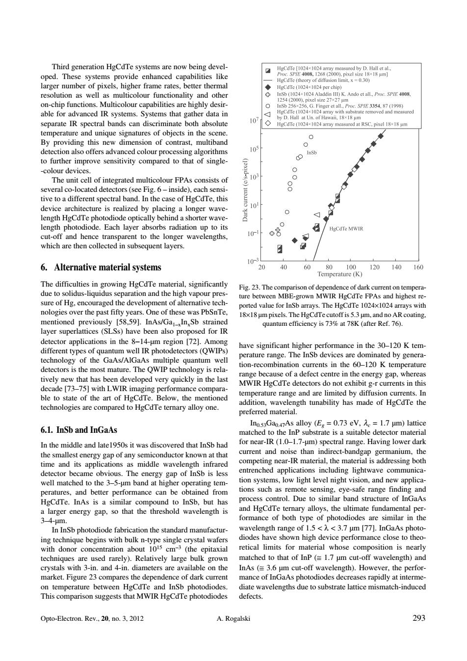
resolution as wel tems.Systems that gather data in 79 separate IR spectral bands can discriminate both absolute 107 8 0 The unit cell of integrated multicolour FPAs consists of 10 8 and In the case of HgCdTe.this architecture is i nger wave 10 CdTe ehin orter wave cut-off and to the longer avee which re then collected in subsequent layers 6.Alternative material system 10 40 60 140 tioned er the pa 58.591.ImAs/Ga-In,Sb pixels.The HgCdTec no AR coating 1the30-120K yof the GaAs/AlGaAs multiple quantum well detectors is the ost mature.The QWIP te rents in the 60-120 K temperature logy is rela Below,the mentioned emperature range and are limited by diffusion cu ents.I e ternary alloy one tunability has made of HgCdTe the 6.1.InSb and InGaAs matched In the middle and late1950s it was discovered that inSb had or near-IR (1.0 ctral range.F 1ng10 the smallest ene onductor kr at tha material is addressing both time an Th incl com tions such as remote sensing. -safe range find and ess control.Due of Inc large renergy gap.so that the threshold wavelength is nSh photodiode fabrication the standard n velength range of 1.5<3.7 um [77].InGaAs photo ing technique begins with bulk n-type single c stal wafer to t with donor co (th ed to that of InP (.7m c )an crystals with 3-in.and 4n diameter s are available on the InAs (=3.6 um cut-off wavelength).However.the perfor market.Figure 23 compar s the dependence of dark curren nance of InGaAs photodio des dec es rapidly at int s aue to s ate lattice mismat induce Opto-Electron.Rev.20.no.3.2012 293 Third generation HgCdTe systems are now being devel− oped. These systems provide enhanced capabilities like larger number of pixels, higher frame rates, better thermal resolution as well as multicolour functionality and other on−chip functions. Multicolour capabilities are highly desir− able for advanced IR systems. Systems that gather data in separate IR spectral bands can discriminate both absolute temperature and unique signatures of objects in the scene. By providing this new dimension of contrast, multiband detection also offers advanced colour processing algorithms to further improve sensitivity compared to that of single− −colour devices. The unit cell of integrated multicolour FPAs consists of several co−located detectors (see Fig. 6 – inside), each sensi− tive to a different spectral band. In the case of HgCdTe, this device architecture is realized by placing a longer wave− length HgCdTe photodiode optically behind a shorter wave− length photodiode. Each layer absorbs radiation up to its cut−off and hence transparent to the longer wavelengths, which are then collected in subsequent layers. 6. Alternative material systems The difficulties in growing HgCdTe material, significantly due to solidus−liquidus separation and the high vapour pres− sure of Hg, encouraged the development of alternative tech− nologies over the past fifty years. One of these was PbSnTe, mentioned previously [58,59]. InAs/Ga1–xInxSb strained layer superlattices (SLSs) have been also proposed for IR detector applications in the 8
14−μm region [72]. Among different types of quantum well IR photodetectors (QWIPs) technology of the GaAs/AlGaAs multiple quantum well detectors is the most mature. The QWIP technology is rela− tively new that has been developed very quickly in the last decade [73–75] with LWIR imaging performance compara− ble to state of the art of HgCdTe. Below, the mentioned technologies are compared to HgCdTe ternary alloy one. 6.1. InSb and InGaAs In the middle and late1950s it was discovered that InSb had the smallest energy gap of any semiconductor known at that time and its applications as middle wavelength infrared detector became obvious. The energy gap of InSb is less well matched to the 3–5−μm band at higher operating tem− peratures, and better performance can be obtained from HgCdTe. InAs is a similar compound to InSb, but has a larger energy gap, so that the threshold wavelength is 3–4−μm. In InSb photodiode fabrication the standard manufactur− ing technique begins with bulk n−type single crystal wafers with donor concentration about 1015 cm–3 (the epitaxial techniques are used rarely). Relatively large bulk grown crystals with 3−in. and 4−in. diameters are available on the market. Figure 23 compares the dependence of dark current on temperature between HgCdTe and InSb photodiodes. This comparison suggests that MWIR HgCdTe photodiodes have significant higher performance in the 30–120 K tem− perature range. The InSb devices are dominated by genera− tion−recombination currents in the 60–120 K temperature range because of a defect centre in the energy gap, whereas MWIR HgCdTe detectors do not exhibit g−r currents in this temperature range and are limited by diffusion currents. In addition, wavelength tunability has made of HgCdTe the preferred material. In0.53Ga0.47As alloy (Eg = 0.73 eV, c = 1.7 μm) lattice matched to the InP substrate is a suitable detector material for near−IR (1.0–1.7−μm) spectral range. Having lower dark current and noise than indirect−bandgap germanium, the competing near−IR material, the material is addressing both entrenched applications including lightwave communica− tion systems, low light level night vision, and new applica− tions such as remote sensing, eye−safe range finding and process control. Due to similar band structure of InGaAs and HgCdTe ternary alloys, the ultimate fundamental per− formance of both type of photodiodes are similar in the wavelength range of 1.5 < < 3.7 μm [77]. InGaAs photo− diodes have shown high device performance close to theo− retical limits for material whose composition is nearly matched to that of InP ( 1.7 μm cut−off wavelength) and InAs ( 3.6 μm cut−off wavelength). However, the perfor− mance of InGaAs photodiodes decreases rapidly at interme− diate wavelengths due to substrate lattice mismatch−induced defects. Opto−Electron. Rev., 20, no. 3, 2012 A. Rogalski 293 Fig. 23. The comparison of dependence of dark current on tempera− ture between MBE−grown MWIR HgCdTe FPAs and highest re− ported value for InSb arrays. The HgCdTe 1024
1024 arrays with 18
18 μm pixels. The HgCdTe cutoff is 5.3 μm, and no AR coating, quantum efficiency is 73% at 78K (after Ref. 76).�