正在加载图片...
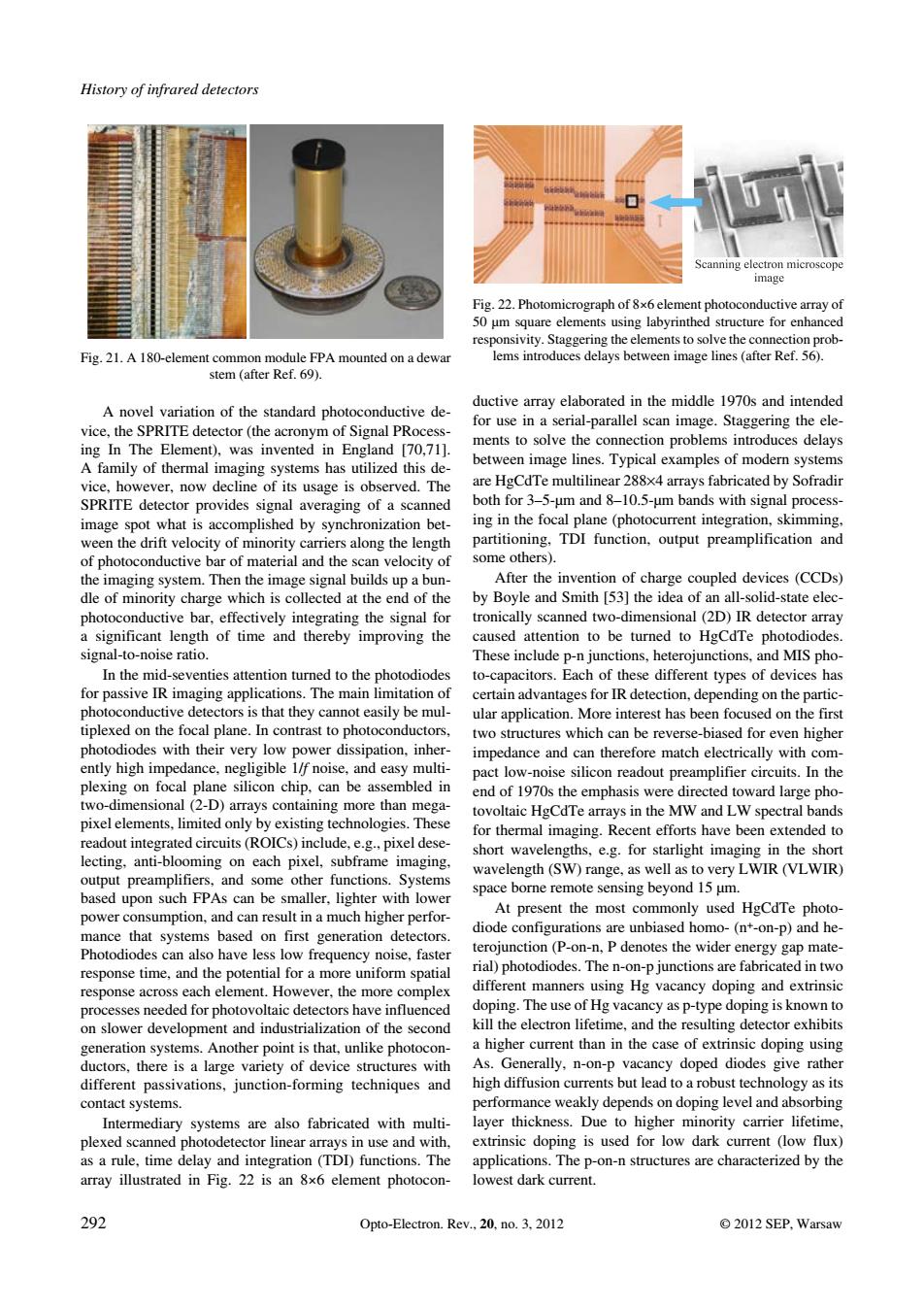
History of infrared detectors ductive array elaborated in the middle 1970s and intended a novel variation of the standard photoconductive de- or use in a serial-parallel scan image.Staggering the ele ments to solve the con pro are HgCdTe multilinear cated by Sofradi of isobserved.The both for35-m and 8-10.5-m bands with signal process ot what isacc lished by svnc ation het long the length ignal After the invention of charge coupled devices (CCDs dle of minority charge which is collected at the end of the by Boyle and Smith [53]the idea of an all-solid-state elec imao-ibe These include,heterojunctions MI pho to-capacitors. Each of these different types of devices ha n a tiplexed on the focal plane.In contrast to photocon ctors two structures which can be reverse-biased for even highe mpedance and can therefore match el ctncally with con its.In th plexing on focal plane silicon chip.cn be mbled in d l ovoltaic HgCdTe arrays in the MW and LW spectral band or thermal imaging.Recent efforts have been extended to (SW light LWIR (VLWIR space bome remote sensing beyond 15 um. At present the most commonly used HgCdTe photo tha Photdiodes n also have less low frequencynoise.faste response time,and th re uni orm spa rent manners using Hg vacancy doping and extrins es needed for photovolta slower developmen kill th p-type dopng is the a hisher current than in the case of extrinsic doping using ductors,there is a large variety of device structures with passivations,junctio high mrally.o-pvacaney doped diodes gve rathe -forming techniques and aky dep Intermediary are also fahricated with multi scaned photodetector linear arrays ns rinsic doping is used for low dark current (low flux 292 Opto-Electron.Rev.n.3.2012 2012 SEP.WarsawA novel variation of the standard photoconductive de− vice, the SPRITE detector (the acronym of Signal PRocess− ing In The Element), was invented in England [70,71]. A family of thermal imaging systems has utilized this de− vice, however, now decline of its usage is observed. The SPRITE detector provides signal averaging of a scanned image spot what is accomplished by synchronization bet− ween the drift velocity of minority carriers along the length of photoconductive bar of material and the scan velocity of the imaging system. Then the image signal builds up a bun− dle of minority charge which is collected at the end of the photoconductive bar, effectively integrating the signal for a significant length of time and thereby improving the signal−to−noise ratio. In the mid−seventies attention turned to the photodiodes for passive IR imaging applications. The main limitation of photoconductive detectors is that they cannot easily be mul− tiplexed on the focal plane. In contrast to photoconductors, photodiodes with their very low power dissipation, inher− ently high impedance, negligible 1/f noise, and easy multi− plexing on focal plane silicon chip, can be assembled in two−dimensional (2−D) arrays containing more than mega− pixel elements, limited only by existing technologies. These readout integrated circuits (ROICs) include, e.g., pixel dese− lecting, anti−blooming on each pixel, subframe imaging, output preamplifiers, and some other functions. Systems based upon such FPAs can be smaller, lighter with lower power consumption, and can result in a much higher perfor− mance that systems based on first generation detectors. Photodiodes can also have less low frequency noise, faster response time, and the potential for a more uniform spatial response across each element. However, the more complex processes needed for photovoltaic detectors have influenced on slower development and industrialization of the second generation systems. Another point is that, unlike photocon− ductors, there is a large variety of device structures with different passivations, junction−forming techniques and contact systems. Intermediary systems are also fabricated with multi− plexed scanned photodetector linear arrays in use and with, as a rule, time delay and integration (TDI) functions. The array illustrated in Fig. 22 is an 8×6 element photocon− ductive array elaborated in the middle 1970s and intended for use in a serial−parallel scan image. Staggering the ele− ments to solve the connection problems introduces delays between image lines. Typical examples of modern systems are HgCdTe multilinear 288
4 arrays fabricated by Sofradir both for 3–5−μm and 8–10.5−μm bands with signal process− ing in the focal plane (photocurrent integration, skimming, partitioning, TDI function, output preamplification and some others). After the invention of charge coupled devices (CCDs) by Boyle and Smith [53] the idea of an all−solid−state elec− tronically scanned two−dimensional (2D) IR detector array caused attention to be turned to HgCdTe photodiodes. These include p−n junctions, heterojunctions, and MIS pho− to−capacitors. Each of these different types of devices has certain advantages for IR detection, depending on the partic− ular application. More interest has been focused on the first two structures which can be reverse−biased for even higher impedance and can therefore match electrically with com− pact low−noise silicon readout preamplifier circuits. In the end of 1970s the emphasis were directed toward large pho− tovoltaic HgCdTe arrays in the MW and LW spectral bands for thermal imaging. Recent efforts have been extended to short wavelengths, e.g. for starlight imaging in the short wavelength (SW) range, as well as to very LWIR (VLWIR) space borne remote sensing beyond 15 μm. At present the most commonly used HgCdTe photo− diode configurations are unbiased homo− (n+−on−p) and he− terojunction (P−on−n, P denotes the wider energy gap mate− rial) photodiodes. The n−on−p junctions are fabricated in two different manners using Hg vacancy doping and extrinsic doping. The use of Hg vacancy as p−type doping is known to kill the electron lifetime, and the resulting detector exhibits a higher current than in the case of extrinsic doping using As. Generally, n−on−p vacancy doped diodes give rather high diffusion currents but lead to a robust technology as its performance weakly depends on doping level and absorbing layer thickness. Due to higher minority carrier lifetime, extrinsic doping is used for low dark current (low flux) applications. The p−on−n structures are characterized by the lowest dark current. History of infrared detectors 292 Opto−Electron. Rev., 20, no. 3, 2012 © 2012 SEP, Warsaw Fig. 21. A 180−element common module FPA mounted on a dewar stem (after Ref. 69). Fig. 22. Photomicrograph of 8×6 element photoconductive array of 50 μm square elements using labyrinthed structure for enhanced responsivity. Staggering the elements to solve the connection prob− lems introduces delays between image lines (after Ref. 56)