正在加载图片...
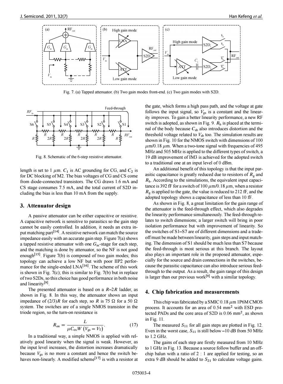
J.Semicond.2011,32(7) Han Kefeng et al. (a) RF (b) High gain mode (c) High gain mode Low gain mode Low gain mode Fig.7.(a)Tapped attenuator.(b)Two gain modes front-end.(c)Two gain modes with S2D Feed-through the gate,which forms a high pass path,and the voltage at gate follows the input signal,so Vgs is a constant and the linear- ity improves.To gain a better linearity performance,a new RF switch is adopted,as shown in Fig.9.R is placed at the termi- nal of the body because Csb also introduces distortion and the threshold voltage related to Vsb too.The simulation results are shown in Fig.10 for the NMOS switch with dimensions of 100 um/0.18 um.When a two-tone signal with frequencies of 495 MHz and 505 MHz is applied to the different types of switch,a Fig.8.Schematic of the 6-step resistive attenuator 19 dB improvement of IM3 is achieved for the adopted switch to a traditional one at an input level of 0 dBm. length is set to 1 um.C is AC grounding for CG,and C2 is An additional benefit of this topology is that the input par- for DC blocking of M2.The bias voltages of CG and CS come asitic capacitance is greatly reduced due to resistors of R.and from diode-connected transistors.The CG draws 1.6 mA and Ro.According to the simulations,the equivalent input capaci- CS stage consumes 7.5 mA,and the total current of S2D in- tance is 392 fF for a switch of 100 um/0.18 um,when a resistor cluding the bias is less than 10 mA from the supply. Re is applied to the gate,the value is reduced to 212 fF,and the adopted topology shows a capacitance of less than 10 fF. 3.Attenuator design As shown in Fig.8,a great limitation for the gain range of the attenuator is the feed-through effect,which also degrades A passive attenuator can be either capacitive or resistive. the linearity performance simultaneously.The feed-through re- A capacitive network is sensitive to parasitics so the gain step lates to switch dimensions;a larger switch will bring in poor cannot be easily controlled.In addition.it needs an extra in- isolation performance but with improvement of linearity.So put matching parA resistive network can match the source the switches of S1-S7 are of different dimensions and a trade- impedance easily with an accurate gain step.Figure 7(a)shows offmust be made between linearity,gain steps and input match- a tapped resistive attenuator with one Gm-stage for each step, ing.The dimension of S1 should be much less than S7 because and the matching is done by attenuator,so the NF is not good the feed-through is most serious at this branch.The layout enoughl15).Figure 7(b)is composed of two gain modes;this also plays an important role in the proposed attenuator,espe- topology can achieve a low NF but with poor IIP2 perfor- cially for the source and drain connections in the switches,be- mance for the single-ended LNA[16].The scheme of this work cause the parasitic capacitance can also introduce serious feed- is shown in Fig.7(c);this is similar to Fig.7(b)but in replace through to the output.As a result,the gain range of this design of two S2Ds,so this choice has good performance in both noise is larger than our previous work]with a similar topology. and linearity] The presented attenuator is based on a R-2R ladder,as 4.Chip fabrication and measurements shown in Fig.8.In this way,the attenuator shows an input impedance of(2/3)R for each step,so R is 75 for a 50 This chip was fabricated by a SMIC 0.18 um 1P6M CMOS system.The switches are of a single NMOS transistor in the process.It accounts for an area of 0.54 mm2 with ESD pro- triode region,so the turn-on resistance is tected PADs and the core area of S2D is 0.06 mm2,as shown L in Fig.11. Ron = (17 The measured S1 for all gain steps are plotted in Fig.12. uCoxW (Vgs -VT) Even in the worst case,S11 is still below-10 dB from 50 MHz In a traditional way,a simple NMOS is applied with rel- to 1.2 GHz. atively good linearity when the signal is weak.However,as The gains of each step are firstly measured from 10 MHz the input level increases,the distortion increases dramatically to I GHz in Fig.13.Because a source follow buffer and an off- because Vgs is no more a constant and hence the switch be- chip balun with a ratio of 2:I are applied for testing,so an haves non-linearly.A modified schemel7l is with a resistor at extra 9 dB should be added to S21 to calculate voltage gains. 075003-4J. Semicond. 2011, 32(7) Han Kefeng et al. Fig. 7. (a) Tapped attenuator. (b) Two gain modes front-end. (c) Two gain modes with S2D. Fig. 8. Schematic of the 6-step resistive attenuator. length is set to 1 m. C1 is AC grounding for CG, and C2 is for DC blocking of M2. The bias voltages of CG and CS come from diode-connected transistors. The CG draws 1.6 mA and CS stage consumes 7.5 mA, and the total current of S2D including the bias is less than 10 mA from the supply. 3. Attenuator design A passive attenuator can be either capacitive or resistive. A capacitive network is sensitive to parasitics so the gain step cannot be easily controlled. In addition, it needs an extra input matching partŒ14. A resistive network can match the source impedance easily with an accurate gain step. Figure 7(a) shows a tapped resistive attenuator with one Gm-stage for each step, and the matching is done by attenuator, so the NF is not good enoughŒ15. Figure 7(b) is composed of two gain modes; this topology can achieve a low NF but with poor IIP2 performance for the single-ended LNAŒ16. The scheme of this work is shown in Fig. 7(c); this is similar to Fig. 7(b) but in replace of two S2Ds, so this choice has good performance in both noise and linearityŒ9 . The presented attenuator is based on a R–2R ladder, as shown in Fig. 8. In this way, the attenuator shows an input impedance of (2/3)R for each step, so R is 75 for a 50 system. The switches are of a single NMOS transistor in the triode region, so the turn-on resistance is Ron D L CoxW Vgs VT : (17) In a traditional way, a simple NMOS is applied with relatively good linearity when the signal is weak. However, as the input level increases, the distortion increases dramatically because Vgs is no more a constant and hence the switch behaves non-linearly. A modified schemeŒ17 is with a resistor at the gate, which forms a high pass path, and the voltage at gate follows the input signal, so Vgs is a constant and the linearity improves. To gain a better linearity performance, a new RF switch is adopted, as shown in Fig. 9. Rb is placed at the terminal of the body because Csb also introduces distortion and the threshold voltage related to Vsb too. The simulation results are shown in Fig. 10 for the NMOS switch with dimensions of 100 m/0.18 m. When a two-tone signal with frequencies of 495 MHz and 505 MHz is applied to the different types of switch, a 19 dB improvement of IM3 is achieved for the adopted switch to a traditional one at an input level of 0 dBm. An additional benefit of this topology is that the input parasitic capacitance is greatly reduced due to resistors of Rg and Rb. According to the simulations, the equivalent input capacitance is 392 fF for a switch of 100 m/0.18 m, when a resistor Rg is applied to the gate, the value is reduced to 212 fF, and the adopted topology shows a capacitance of less than 10 fF. As shown in Fig. 8, a great limitation for the gain range of the attenuator is the feed-through effect, which also degrades the linearity performance simultaneously. The feed-through relates to switch dimensions; a larger switch will bring in poor isolation performance but with improvement of linearity. So the switches of S1–S7 are of different dimensions and a tradeoff must be made between linearity, gain steps and input matching. The dimension of S1 should be much less than S7 because the feed-through is most serious at this branch. The layout also plays an important role in the proposed attenuator, especially for the source and drain connections in the switches, because the parasitic capacitance can also introduce serious feedthrough to the output. As a result, the gain range of this design is larger than our previous workŒ9 with a similar topology. 4. Chip fabrication and measurements This chip was fabricated by a SMIC 0.18m 1P6M CMOS process. It accounts for an area of 0.54 mm2 with ESD protected PADs and the core area of S2D is 0.06 mm2 , as shown in Fig. 11. The measured S11 for all gain steps are plotted in Fig. 12. Even in the worst case, S11 is still below –10 dB from 50 MHz to 1.2 GHz. The gains of each step are firstly measured from 10 MHz to 1 GHz in Fig. 13. Because a source follow buffer and an offchip balun with a ratio of 2 : 1 are applied for testing, so an extra 9 dB should be added to S21 to calculate voltage gains. 075003-4