正在加载图片...

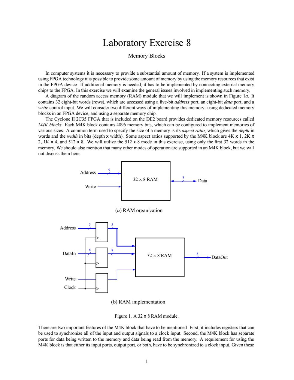
Laboratory Exercise 8 Memory Blocks Incmpuer systems it isnecesary to provide a substantial amount of memory.Ifa system is implemented n the EpGA to prov chips to the FPGA.In this exercise we will examine the general issues involved in impementing such memorv A diagram of the random access memory (RAM)module that we will implement is shown in Figure la.It contains 32 ight-b (rows),which ar re accessed using a five-bit add ort.and a blocks inn FPGA devi cated memory and using The Cyclone II 2C35 FPGA that is included on the DE2 board provides dedicated memory resources called Each M4K block contan 0 mmry bits.which can be confgured to ze or e4KL2K 2.IKand 5128.We will utilize the 512 mode in this exercise,using only the first 32 words in the memory.We should also mention that many other modes of operation are supported in an M4K block,but we will not discuss them here Address_5 32 x 8 RAM Data Write (a)RAM organization 32x8 RAM 8 DataOut (b)RAM implementation Figure 1.A 32x8 RAM module. s for data being written to the memoryand data beingread from M4K block is that ether its input ports,ouput portor both,have to be synchronedtoa ock input.Given theseLaboratory Exercise 8 Memory Blocks In computer systems it is necessary to provide a substantial amount of memory. If a system is implemented using FPGA technology it is possible to provide some amount of memory by using the memory resources that exist in the FPGA device. If additional memory is needed, it has to be implemented by connecting external memory chips to the FPGA. In this exercise we will examine the general issues involved in implementing such memory. A diagram of the random access memory (RAM) module that we will implement is shown in Figure 1a. It contains 32 eight-bit words (rows), which are accessed using a five-bit address port, an eight-bit data port, and a write control input. We will consider two different ways of implementing this memory: using dedicated memory blocks in an FPGA device, and using a separate memory chip. The Cyclone II 2C35 FPGA that is included on the DE2 board provides dedicated memory resources called M4K blocks. Each M4K block contains 4096 memory bits, which can be configured to implement memories of various sizes. A common term used to specify the size of a memory is its aspect ratio, which gives the depth in words and the width in bits (depth x width). Some aspect ratios supported by the M4K block are 4K x 1, 2K x 2, 1K x 4, and 512 x 8. We will utilize the 512 x 8 mode in this exercise, using only the first 32 words in the memory. We should also mention that many other modes of operation are supported in an M4K block, but we will not discuss them here. 32 x 8 RAM Write 5 Address 8 Data (a) RAM organization 32 x 8 RAM 8 DataOut 5 Address 8 DataIn Write Clock 5 8 (b) RAM implementation Figure 1. A 32 x 8 RAM module. There are two important features of the M4K block that have to be mentioned. First, it includes registers that can be used to synchronize all of the input and output signals to a clock input. Second, the M4K block has separate ports for data being written to the memory and data being read from the memory. A requirement for using the M4K block is that either its input ports, output port, or both, have to be synchronized to a clock input. Given these 1