正在加载图片...
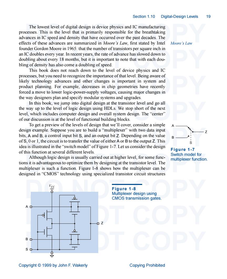
Section1.10 Digital-Design Levels 9 The lowest level of digital design is device physics and IC manufacturing processes.This is the level that is primarily responsible for the breathtaking advances in IC speed and density that have occurred over the past decades.The effects of these advances are summarized in Moore's Law,first stated by Intel Moore's Law founder Gordon Moore in 1965:that the number of transistors per square inch in an IC doubles every year.In recent years,the rate ofadvance has slowed down to doubling about every 18 months,bu it is important to note that with each ou bling of density has also come a doubling of speed. This book does not reach down to the level of device physics and IC but the importance of thatevel.Being aware of likely technology advances and other changes is important in system and product planning.For example,decreases in chip geometries have recently lar systems and upgrades In this book,we jump into digital design at the transistor level and go all the way up to the level of logic design using HDLs.We stop short of the next evel,which includes computer design and overall system design.The “center of our discussion is at the level of functional building blocks. To get a preview of the levels of design that we'll cover,consider a simple A design example.Suppose you are to build a"multiplexer"with two data input bits,A and B.a control input bitS,and an output bit Z.Depending on the value ofS,0 or 1,the circuit is to transfer the value of either A or B to the output Z.This c idea is illustrated in the"switch model"of Figure 1-7.Let us consider the design of this functio n at seve eral different levels Figure 1-7 Although logic design is usually carried out at higher level,for some func- lel for tions it is advantageous to optimize them by designing at the transistor level.The multiplexer is such a function.Figure 1-8 shows how the multiplexer can be designed in"CMOS"technology using specialized transistor circuit structures Figure 1-8 Multiplexer design using CMOS transmission gates. COPY Copyright 1999 by John F.Wakerly Copying ProhibitedSection 1.10 Digital-Design Levels 19 DO NOT COPY DO NOT COPY DO NOT COPY DO NOT COPY DO NOT COPY DO NOT COPY DO NOT COPY DO NOT COPY DO NOT COPY Copyright © 1999 by John F. Wakerly Copying Prohibited The lowest level of digital design is device physics and IC manufacturing processes. This is the level that is primarily responsible for the breathtaking advances in IC speed and density that have occurred over the past decades. The effects of these advances are summarized in Moore’s Law, first stated by Intel founder Gordon Moore in 1965: that the number of transistors per square inch in an IC doubles every year. In recent years, the rate of advance has slowed down to doubling about every 18 months, but it is important to note that with each doubling of density has also come a doubling of speed. This book does not reach down to the level of device physics and IC processes, but you need to recognize the importance of that level. Being aware of likely technology advances and other changes is important in system and product planning. For example, decreases in chip geometries have recently forced a move to lower logic-power-supply voltages, causing major changes in the way designers plan and specify modular systems and upgrades. In this book, we jump into digital design at the transistor level and go all the way up to the level of logic design using HDLs. We stop short of the next level, which includes computer design and overall system design. The “center” of our discussion is at the level of functional building blocks. To get a preview of the levels of design that we’ll cover, consider a simple design example. Suppose you are to build a “multiplexer” with two data input bits, A and B, a control input bit S, and an output bit Z. Depending on the value of S, 0 or 1, the circuit is to transfer the value of either A or B to the output Z. This idea is illustrated in the “switch model” of Figure 1-7. Let us consider the design of this function at several different levels. Although logic design is usually carried out at higher level, for some functions it is advantageous to optimize them by designing at the transistor level. The multiplexer is such a function. Figure 1-8 shows how the multiplexer can be designed in “CMOS” technology using specialized transistor circuit structures Moore’s Law A B Z S Figure 1-7 Switch model for multiplexer function. A B S VCC Z Figure 1-8 Multiplexer design using CMOS transmission gates