正在加载图片...
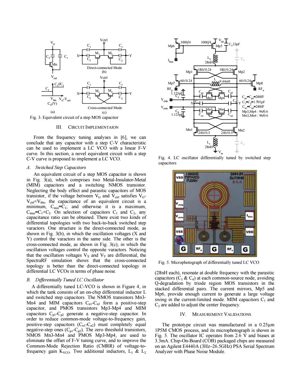
,1000/4 1000/4 C,23pF 28nH Direct-connected Mode 6) 180/0.24 180/0.241 Mpl Mp2 60/0.24 60/0.24 C nc Mp7 20024a Mp8 RF 3 C=C=288 V图 Y C=C,=1.701pF Cross-connected Mode C=C=288 (a) (c) 学 Mp3,Mp4:96/0.6 Fig.3.Equivalent circuit of a step MOS capacitor Mn3,Mn4:96/0.6 III.CIRCUIT IMPLEMENTAION Mnl Mn2 240/0.5 240/0.5 From the frequency tuning analyses in 6],we can conclude that any capacitor with a step C-V characteristic can be used to implement a LC VCO with a linear F-V 28n curve.In this section,a novel equivalent circuit with a step C-V curve is proposed to implement a LC VCO. Fig.4.LC oscillator differentially tuned by switched step capacitors A.Switched Step Capacitors An equivalent circuit of a step MOS capacitor is shown 20042到 in Fig.3(a),which comprises two Metal-Insulator-Metal 2T0 (MIM)capacitors and a switching NMOS transistor. Neglecting the body effect and parasitic capacitors of MOS transistor,if the voltage between VG and Verl satisfies VG- Vet<Vthn,the capacitance of an equivalent circuit is a minimum,Cmin=C1;and otherwise it is a maximum, Cmax=CI+C2.On selection of capacitors Cl and C2.any capacitance ratio can be obtained.There exist two kinds of differential topologies with two back-to-back switched step varactors.One structure is the direct-connected mode,as shown in Fig.3(b),in which the oscillation voltages (X and Y)control the varactors in the same side.The other is the cross-connected mode,as shown in Fig.3(c),in which the oscillation voltages control the opposite varactors.Noticing RFp G RF that the oscillation voltages Vx and Vy are differential,the SpectraRF simulation shows that the cross-connected Fig.5.Microphotograph of differentially tuned LC VCO topology is better than the direct-connected topology in differential LC VCOs in terms of phase noise. (28nH each),resonate at double frequency with the parasitic B.Differentially Tuned LC Oscillator capacitors (C:Ca)at each common-source node,avoiding A differentially tuned LC-VCO is shown in Figure 4,in Q-degradation by triode region MOS transistors in the which the tank consists of an on-chip differential inductor L stacked differential pairs.The current mirrors,Mp5 and and switched step capacitors.The NMOS transistors Mn3- Mp6,provide enough current to generate a large voltage swing in the current-limited mode.MIM capacitors C and Mn4 and MIM capacitors Cni-Cn2 form a positive-step capacitor,and PMOS transistors Mp3-Mp4 and MIM C2 are added to adjust the center frequency. capacitors Cpl-Cp2 generate a negative-step capacitor.In IV.MEASUREMENT VALIDATIONS order to reduce common-mode voltage-to-frequency gain, positive-step capacitors (CnI-Cn2)must completely equal The prototype circuit was manufactured in a 0.25um negative-step ones(CpI-Cp2).The zero threshold transistors, 1P5M CMOS process,and its microphotograph is shown in NMOS Mn3-Mn4 and PMOS Mp3-Mp4,are used to Fig.5.The oscillator IC operates from 2.6 V and biases at eliminate the offset of F-V tuning curve,and to improve the 3.3mA.Chip-On-Board(COB)packaged chips are measured Common-Mode Rejection Ratio (CMRR)of voltage-to- on an Agilent E4440A(3Hz~26.5GHz)PSA Serial Spectrum frequency gain Kvco.Two additional inductors,LI&L2 Analyzer with Phase Noise Module.III. CIRCUIT IMPLEMENTAION From the frequency tuning analyses in [6], we can conclude that any capacitor with a step C-V characteristic can be used to implement a LC VCO with a linear F-V curve. In this section, a novel equivalent circuit with a step C-V curve is proposed to implement a LC VCO. A. Switched Step Capacitors An equivalent circuit of a step MOS capacitor is shown in Fig. 3(a), which comprises two Metal-Insulator-Metal (MIM) capacitors and a switching NMOS transistor. Neglecting the body effect and parasitic capacitors of MOS transistor, if the voltage between VG and Vctrl satisfies VGVctrl<Vthn, the capacitance of an equivalent circuit is a minimum, Cmin=C1; and otherwise it is a maximum, Cmax=C1+C2. On selection of capacitors C1 and C2, any capacitance ratio can be obtained. There exist two kinds of differential topologies with two back-to-back switched step varactors. One structure is the direct-connected mode, as shown in Fig. 3(b), in which the oscillation voltages (X and Y) control the varactors in the same side. The other is the cross-connected mode, as shown in Fig. 3(c), in which the oscillation voltages control the opposite varactors. Noticing that the oscillation voltages VX and VY are differential, the SpectraRF simulation shows that the cross-connected topology is better than the direct-connected topology in differential LC VCOs in terms of phase noise. B. Differentially Tuned LC Oscillator A differentially tuned LC-VCO is shown in Figure 4, in which the tank consists of an on-chip differential inductor L and switched step capacitors. The NMOS transistors Mn3- Mn4 and MIM capacitors Cn1-Cn2 form a positive-step capacitor, and PMOS transistors Mp3-Mp4 and MIM capacitors Cp1-Cp2 generate a negative-step capacitor. In order to reduce common-mode voltage-to-frequency gain, positive-step capacitors (Cn1-Cn2) must completely equal negative-step ones (Cp1-Cp2). The zero threshold transistors, NMOS Mn3-Mn4 and PMOS Mp3-Mp4, are used to eliminate the offset of F-V tuning curve, and to improve the Common-Mode Rejection Ratio (CMRR) of voltage-tofrequency gain KVCO. Two additional inductors, L1 & L2 (28nH each), resonate at double frequency with the parasitic capacitors (C3 & C4) at each common-source node, avoiding Q-degradation by triode region MOS transistors in the stacked differential pairs. The current mirrors, Mp5 and Mp6, provide enough current to generate a large voltage swing in the current-limited mode. MIM capacitors C1 and C2 are added to adjust the center frequency. IV. MEASUREMENT VALIDATIONS The prototype circuit was manufactured in a 0.25µm 1P5M CMOS process, and its microphotograph is shown in Fig. 5. The oscillator IC operates from 2.6 V and biases at 3.3mA. Chip-On-Board (COB) packaged chips are measured on an Agilent E4440A (3Hz~26.5GHz) PSA Serial Spectrum Analyzer with Phase Noise Module. C1 //C2 C1 Vthn VG-Vctrl CV(V) Mn C C2 1 Vctrl VG C2 C2 X Y C2 C2 X Y Vctrl Vctrl C1 C1 C1 C1 M1 M2 M1 M2 Direct-connected Mode Cross-connected Mode (a) (c) (b) Fig. 3. Equivalent circuit of a step MOS capacitor Mn1 Mn2 Mp1 Mp2 L Vdd Vss X Y C1 Cp1 Cn1 C2 Cp2 Cn2 Mn3 Mn4 Mp3 Mp4 Vctrlp Vctrln Mp5 RFp RFn I bias L1 C3 L2 C4 C6 C5 Mp6 Mp7 Mp8 1000 4 1000 4 28nH 28nH 180/ 0.24 180/ 0.24 240/ 0.5 240/0.5 60/ 0.24 9.44nH 60/0.24 Cp1=Cp2=288fF C1 =C2 =1.701pF Cn1=Cn2=288fF Mp3,Mp4 : 96/0.6 Mn3,Mn4 : 96/0.6 1.125pF 1.125pF C7 23pF Fig. 4. LC oscillator differentially tuned by switched step capacitors Fig. 5. Microphotograph of differentially tuned LC VCO