正在加载图片...
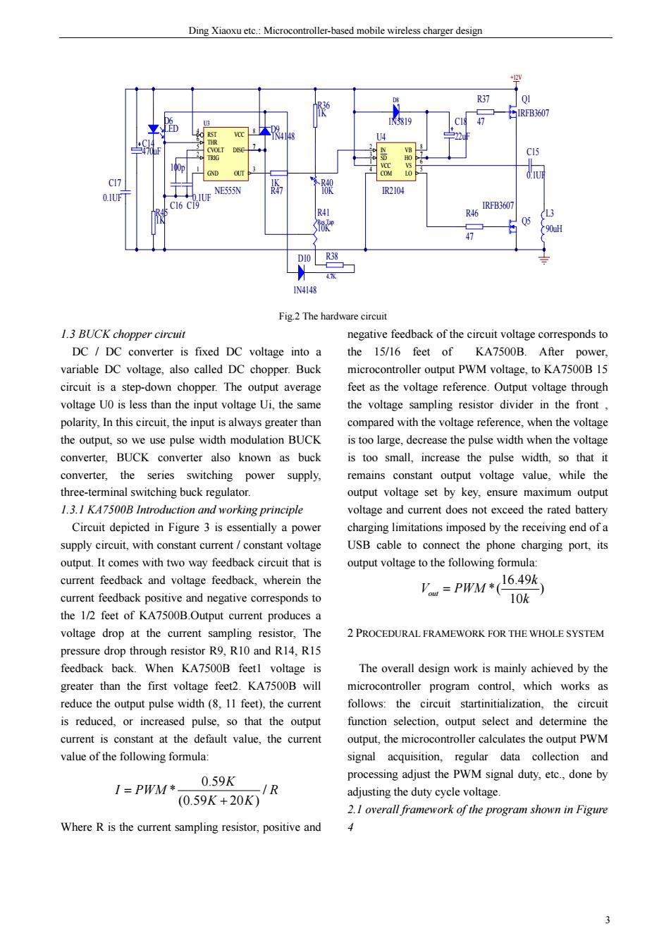
Ding Xiaoxu ete.:Microcontroller-based mobile wireless charger design 一RB360 R210 DI0 R38 N4148 Fig 2 The hardware circuit 1.3 BUCK chopper circui negative feedback of the DC/DC converter is fixed DC voltage into a the 15/16 feet of KA7500B.After power variable DC voltage,also called DC chopper.Buck microcontroller output PWM voltage,to KA7500B 15 circuit is a step-down chopper.The output average feet as the voltage reference.Output voltage through voltage Uo is less than the input voltage Ui.the same the voltage sampling resistor divider in the front compared with the voltage reference.when the voltage is too large.decrease the puse width when the voltae converter.BUCK converter also known as buck is too small,increase the pulse width,so that it converter,the series switching power supply, remains constant output voltage value.while the three-terminal switching buck regulator. output voltage set by key,ensure maximum output 1.3.I KA7500B Introduction and working principle voltage and current does not exceed the rated battery Circuit depicted in Figure3 is essentiallya powe supply circuit,with constant current/constant voltage output.It comes with two way feedback circuit that is output voltage to the following formula current feedback and voltage feedback.wherein the current feedback positive and negative corresponds to '=PwWM◆6.49k 10k the 1/2 feet of KA7500B.Outpu current pro voltage drop at the current sampling resistor The 2 PROCEDURAL FRAMEWORK FOR THE WHOLE SYSTEM pressure drop through resistor R9,R10 and R14,R15 feedback back.When KA7500B feetl voltage is The overall design work is mainly achieved by the greater than the first voltage feet2.KA7500B will microcontroller program control.which works as reduce the output pulse width (811 feet),the current follows:the ciruit startinitialization,the circuit is reduced,or increas tha the oupu funct seection output select and determine th current is constant at the default value,the curren output,the microcontroller calculates the output PWM value of the following formula: signal acquisition,regular data collection and 0.59K processing adjust the PWM signal duty,etc.,done by I=PWM* 0.59K+20/R adjusting the duty cycle voltage 2.1overall framework of the program shownin Figure Where R is the current sampling resistor,positive and 3Ding Xiaoxu etc.: Microcontroller-based mobile wireless charger design 3 TRIG 2 OUT 3 RST 4 CVOLT 5 THR 6 DISC 7 VCC 8 GND 1 U3 NE555N +12V C19 0.1UF C16 100p R36 1K R47 1K R38 4.7K Q5 IRFB3607 Q1 IRFB3607 R37 47 R46 47 C15 0.1UF 90uH L3 C14 470uF R45 1K D6 LED R40 10K VCC 1 COM 4 VB 8 HO 7 VS 6 LO 5 IN 2 SD 3 U4 IR2104 D8 1N5819 C18 22uF C17 0.1UF 10K R41 Res Tap D9 1N4148 D10 1N4148 Fig.2 The hardware circuit 1.3 BUCK chopper circuit DC / DC converter is fixed DC voltage into a variable DC voltage, also called DC chopper. Buck circuit is a step-down chopper. The output average voltage U0 is less than the input voltage Ui, the same polarity, In this circuit, the input is always greater than the output, so we use pulse width modulation BUCK converter, BUCK converter also known as buck converter, the series switching power supply, three-terminal switching buck regulator. 1.3.1 KA7500B Introduction and working principle Circuit depicted in Figure 3 is essentially a power supply circuit, with constant current / constant voltage output. It comes with two way feedback circuit that is current feedback and voltage feedback, wherein the current feedback positive and negative corresponds to the 1/2 feet of KA7500B.Output current produces a voltage drop at the current sampling resistor, The pressure drop through resistor R9, R10 and R14, R15 feedback back. When KA7500B feet1 voltage is greater than the first voltage feet2. KA7500B will reduce the output pulse width (8, 11 feet), the current is reduced, or increased pulse, so that the output current is constant at the default value, the current value of the following formula: 0.59 * / (0.59 20 ) K I PWM R K K = + Where R is the current sampling resistor, positive and negative feedback of the circuit voltage corresponds to the 15/16 feet of KA7500B. After power, microcontroller output PWM voltage, to KA7500B 15 feet as the voltage reference. Output voltage through the voltage sampling resistor divider in the front , compared with the voltage reference, when the voltage is too large, decrease the pulse width when the voltage is too small, increase the pulse width, so that it remains constant output voltage value, while the output voltage set by key, ensure maximum output voltage and current does not exceed the rated battery charging limitations imposed by the receiving end of a USB cable to connect the phone charging port, its output voltage to the following formula: 16.49 *( ) 10 out k V PWM k = 2 PROCEDURAL FRAMEWORK FOR THE WHOLE SYSTEM The overall design work is mainly achieved by the microcontroller program control, which works as follows: the circuit startinitialization, the circuit function selection, output select and determine the output, the microcontroller calculates the output PWM signal acquisition, regular data collection and processing adjust the PWM signal duty, etc., done by adjusting the duty cycle voltage. 2.1 overall framework of the program shown in Figure 4