正在加载图片...
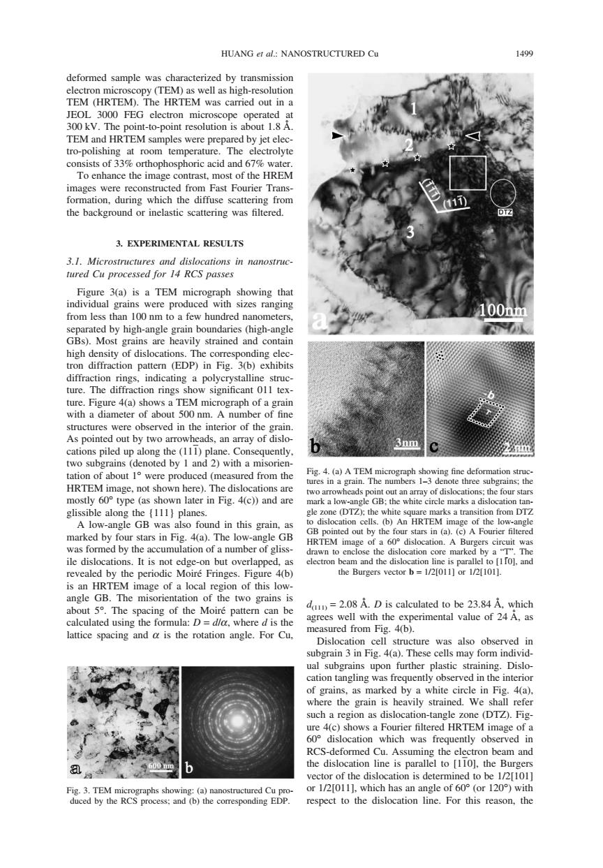
HUANG et al:NANOSTRUCTURED Cu 1499 deformed sample was characterized by transmission electron microscopy (TEM)as well as high-resolution TEM (HRTEM).The HRTEM was carried out in a JEOL 3000 FEG electron microscope operated at 300 kV.The point-to-point resolution is about 1.8 A. TEM and HRTEM samples were prepared by jet elec- tro-polishing at room temperature.The electrolyte consists of 33%orthophosphoric acid and 67%water. To enhance the image contrast,most of the HREM images were reconstructed from Fast Fourier Trans- formation,during which the diffuse scattering from the background or inelastic scattering was filtered. DTZ 3.EXPERIMENTAL RESULTS 3.1.Microstructures and dislocations in nanostruc- tured Cu processed for 14 RCS passes Figure 3(a)is a TEM micrograph showing that individual grains were produced with sizes ranging from less than 100 nm to a few hundred nanometers, 100nm separated by high-angle grain boundaries(high-angle GBs).Most grains are heavily strained and contain high density of dislocations.The corresponding elec- tron diffraction pattern (EDP)in Fig.3(b)exhibits diffraction rings,indicating a polycrystalline struc- ture.The diffraction rings show significant 011 tex- ture.Figure 4(a)shows a TEM micrograph of a grain with a diameter of about 500 nm.A number of fine structures were observed in the interior of the grain. As pointed out by two arrowheads,an array of dislo- 3nm cations piled up along the (111)plane.Consequently, two subgrains (denoted by I and 2)with a misorien- tation of about 1 were produced(measured from the Fig.4.(a)A TEM micrograph showing fine deformation struc- tures in a grain.The numbers 1-3 denote three subgrains:the HRTEM image,not shown here).The dislocations are two arrowheads point out an array of dislocations:the four stars mostly 60 type (as shown later in Fig.4(c))and are mark a low-angle GB:the white circle marks a dislocation tan- glissible along the (111}planes. gle zone (DTZ):the white square marks a transition from DTZ A low-angle GB was also found in this grain,as to dislocation cells.(b)An HRTEM image of the low-angle GB pointed out by the four stars in (a).(c)A Fourier filtered marked by four stars in Fig.4(a).The low-angle GB HRTEM image of a 60 dislocation.A Burgers circuit was was formed by the accumulation of a number of gliss- drawn to enclose the dislocation core marked by a "T".The ile dislocations.It is not edge-on but overlapped,as electron beam and the dislocation line is parallel to [11O].and revealed by the periodic Moire Fringes.Figure 4(b) the Burgers vector b =1/2[011]or 1/2[101]. is an HRTEM image of a local region of this low- angle GB.The misorientation of the two grains is about 5.The spacing of the Moire pattern can be d=2.08 A.D is calculated to be 23.84 A.which calculated using the formula:D=d/o,where d is the agrees well with the experimental value of 24 A,as measured from Fig.4(b). lattice spacing and a is the rotation angle.For Cu. Dislocation cell structure was also observed in subgrain 3 in Fig.4(a).These cells may form individ- ual subgrains upon further plastic straining.Dislo- cation tangling was frequently observed in the interior of grains,as marked by a white circle in Fig.4(a). where the grain is heavily strained.We shall refer such a region as dislocation-tangle zone (DTZ).Fig- ure 4(c)shows a Fourier filtered HRTEM image of a 60 dislocation which was frequently observed in RCS-deformed Cu.Assuming the electron beam and the dislocation line is parallel to [110].the Burgers vector of the dislocation is determined to be 1/2[101] Fig.3.TEM micrographs showing:(a)nanostructured Cu pro- or 1/210111.which has an angle of 60(or 120)with duced by the RCS process:and (b)the corresponding EDP. respect to the dislocation line.For this reason,theHUANG et al.: NANOSTRUCTURED Cu 1499 deformed sample was characterized by transmission electron microscopy (TEM) as well as high-resolution TEM (HRTEM). The HRTEM was carried out in a JEOL 3000 FEG electron microscope operated at 300 kV. The point-to-point resolution is about 1.8 A˚ . TEM and HRTEM samples were prepared by jet electro-polishing at room temperature. The electrolyte consists of 33% orthophosphoric acid and 67% water. To enhance the image contrast, most of the HREM images were reconstructed from Fast Fourier Transformation, during which the diffuse scattering from the background or inelastic scattering was filtered. 3. EXPERIMENTAL RESULTS 3.1. Microstructures and dislocations in nanostructured Cu processed for 14 RCS passes Figure 3(a) is a TEM micrograph showing that individual grains were produced with sizes ranging from less than 100 nm to a few hundred nanometers, separated by high-angle grain boundaries (high-angle GBs). Most grains are heavily strained and contain high density of dislocations. The corresponding electron diffraction pattern (EDP) in Fig. 3(b) exhibits diffraction rings, indicating a polycrystalline structure. The diffraction rings show significant 011 texture. Figure 4(a) shows a TEM micrograph of a grain with a diameter of about 500 nm. A number of fine structures were observed in the interior of the grain. As pointed out by two arrowheads, an array of dislocations piled up along the (111) plane. Consequently, two subgrains (denoted by 1 and 2) with a misorientation of about 1° were produced (measured from the HRTEM image, not shown here). The dislocations are mostly 60° type (as shown later in Fig. 4(c)) and are glissible along the {111} planes. A low-angle GB was also found in this grain, as marked by four stars in Fig. 4(a). The low-angle GB was formed by the accumulation of a number of glissile dislocations. It is not edge-on but overlapped, as revealed by the periodic Moire´ Fringes. Figure 4(b) is an HRTEM image of a local region of this lowangle GB. The misorientation of the two grains is about 5°. The spacing of the Moire´ pattern can be calculated using the formula: D = d/a, where d is the lattice spacing and a is the rotation angle. For Cu, Fig. 3. TEM micrographs showing: (a) nanostructured Cu produced by the RCS process; and (b) the corresponding EDP. Fig. 4. (a) A TEM micrograph showing fine deformation structures in a grain. The numbers 1–3 denote three subgrains; the two arrowheads point out an array of dislocations; the four stars mark a low-angle GB; the white circle marks a dislocation tangle zone (DTZ); the white square marks a transition from DTZ to dislocation cells. (b) An HRTEM image of the low-angle GB pointed out by the four stars in (a). (c) A Fourier filtered HRTEM image of a 60° dislocation. A Burgers circuit was drawn to enclose the dislocation core marked by a “T”. The electron beam and the dislocation line is parallel to [11¯0], and the Burgers vector b = 1/2[011] or 1/2[101]. d(111) = 2.08 A˚ . D is calculated to be 23.84 A˚ , which agrees well with the experimental value of 24 A˚ , as measured from Fig. 4(b). Dislocation cell structure was also observed in subgrain 3 in Fig. 4(a). These cells may form individual subgrains upon further plastic straining. Dislocation tangling was frequently observed in the interior of grains, as marked by a white circle in Fig. 4(a), where the grain is heavily strained. We shall refer such a region as dislocation-tangle zone (DTZ). Figure 4(c) shows a Fourier filtered HRTEM image of a 60° dislocation which was frequently observed in RCS-deformed Cu. Assuming the electron beam and the dislocation line is parallel to [110], the Burgers vector of the dislocation is determined to be 1/2[101] or 1/2[011], which has an angle of 60° (or 120°) with respect to the dislocation line. For this reason, the