正在加载图片...
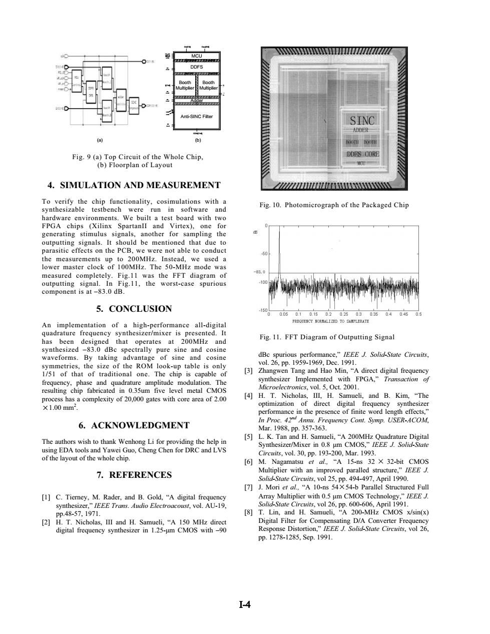
MCU DDFS Booth Booth Multiplie Anti-SINC Filter SINC ADDER ⊙ b) Fig.9(a)Top Circuit of the Whole Chip, DDES CORE (b)Floorplan of Layout 4.SIMULATION AND MEASUREMENT To verify the chip functionality,cosimulations with a Fig.10.Photomicrograph of the Packaged Chip synthesizable testbench were run in software and hardware environments.We built a test board with two FPGA chips (Xilinx SpartanII and Virtex),one for generating stimulus signals,another for sampling the outputting signals.It should be mentioned that due to parasitic effects on the PCB,we were not able to conduct 50 the measurements up to 200MHz.Instead,we used a lower master clock of 100MHz.The 50-MHz mode was 83.0 measured completely.Fig.11 was the FFT diagram of outputting signal.In Fig.11,the worst-case spurious 100 component is at-83.0 dB 5.CONCLUSION 0.050.10.150.20.25030.350.4 049 FREQUENCY NORMALIZED TO SAMPLERATE An implementation of a high-performance all-digital quadrature frequency synthesizer/mixer is presented.It Fig.11.FFT Diagram of Outputting Signal has been designed that operates at 200MHz and synthesized-83.0 dBc spectrally pure sine and cosine waveforms.By taking advantage of sine and cosine dBc spurious performance,"IEEE J.Solid-State Circuits, symmetries,the size of the ROM look-up table is only vol.26,pp.1959-1969,Dec.1991. 1/51 of that of traditional one.The chip is capable of [3]Zhangwen Tang and Hao Min,"A direct digital frequency frequency,phase and quadrature amplitude modulation.The synthesizer Implemented with FPGA,"Transaction of resulting chip fabricated in 0.35um five level metal CMOS Microelectronics,vol.5,Oct.2001. process has a complexity of 20,000 gates with core area of 2.00 [4]H.T.Nicholas,III,H.Samueli,and B.Kim,"The ×1.00mm2 optimization of direct digital frequency synthesizer performance in the presence of finite word length effects," 6.ACKNOWLEDGMENT In Proc.42d Annu.Frequency Cont.Symp.USER-ACOM, Mar.1988,pp.357-363. [5]L.K.Tan and H.Samueli,"A 200MHz Quadrature Digital The authors wish to thank Wenhong Li for providing the help in Synthesizer/Mixer in 0.8 um CMOS,"IEEE J.Solid-State using EDA tools and Yawei Guo,Cheng Chen for DRC and LVS Circuits,vol.30,pp.193-200,Mar.1993. of the layout of the whole chip. [6 M.Nagamatsu et al.,"A 15-ns 32 X 32-bit CMOS Multiplier with an improved paralled structure,"/EEEJ. 7.REFERENCES Solid-State Circuits,vol 25,pp.494-497,April 1990. [7]J.Mori et al.,"A 10-ns 54X54-b Parallel Structured Full [1]C.Tierney,M.Rader,and B.Gold,"A digital frequency Array Multiplier with 0.5 um CMOS Technology,"IEEEJ synthesizer,"IEEE Trans.Audio Electroacoust,vol.AU-19, Solid-State Circuits,vol 26,pp.600-606,April 1991. pp.48-57,1971. [8]T.Lin,and H.Samueli,"A 200-MHz CMOS x/sin(x) [2]H.T.Nicholas,III and H.Samueli,"A 150 MHz direct Digital Filter for Compensating D/A Converter Frequency digital frequency synthesizer in 1.25-um CMOS with-90 Response Distortion,"IEEE J.Solid-State Circuits,vol 26. pp.1278-1285,Sep.1991. I-44. SIMULATION AND MEASUREMENT To verify the chip functionality, cosimulations with a synthesizable testbench were run in software and hardware environments. We built a test board with two FPGA chips (Xilinx SpartanII and Virtex), one for generating stimulus signals, another for sampling the outputting signals. It should be mentioned that due to parasitic effects on the PCB, we were not able to conduct the measurements up to 200MHz. Instead, we used a lower master clock of 100MHz. The 50-MHz mode was measured completely. Fig.11 was the FFT diagram of outputting signal. In Fig.11, the worst-case spurious component is at –83.0 dB. 5. CONCLUSION An implementation of a high-performance all-digital quadrature frequency synthesizer/mixer is presented. It has been designed that operates at 200MHz and synthesized –83.0 dBc spectrally pure sine and cosine waveforms. By taking advantage of sine and cosine symmetries, the size of the ROM look-up table is only 1/51 of that of traditional one. The chip is capable of frequency, phase and quadrature amplitude modulation. The resulting chip fabricated in 0.35um five level metal CMOS process has a complexity of 20,000 gates with core area of 2.00 ᱢ1.00 mm2 . 6. ACKNOWLEDGMENT The authors wish to thank Wenhong Li for providing the help in using EDA tools and Yawei Guo, Cheng Chen for DRC and LVS of the layout of the whole chip. 7. REFERENCES [1] C. Tierney, M. Rader, and B. Gold, “A digital frequency synthesizer,” IEEE Trans. Audio Electroacoust, vol. AU-19, pp.48-57, 1971. [2] H. T. Nicholas, III and H. Samueli, “A 150 MHz direct digital frequency synthesizer in 1.25-µm CMOS with –90 dBc spurious performance,” IEEE J. Solid-State Circuits, vol. 26, pp. 1959-1969, Dec. 1991. [3] Zhangwen Tang and Hao Min, “A direct digital frequency synthesizer Implemented with FPGA,” Transaction of Microelectronics, vol. 5, Oct. 2001. [4] H. T. Nicholas, III, H. Samueli, and B. Kim, “The optimization of direct digital frequency synthesizer performance in the presence of finite word length effects,” In Proc. 42nd Annu. Frequency Cont. Symp. USER-ACOM, Mar. 1988, pp. 357-363. [5] L. K. Tan and H. Samueli, “A 200MHz Quadrature Digital Synthesizer/Mixer in 0.8 µm CMOS,” IEEE J. Solid-State Circuits, vol. 30, pp. 193-200, Mar. 1993. [6] M. Nagamatsu et al., “A 15-ns 32 h 32-bit CMOS Multiplier with an improved paralled structure,” IEEE J. Solid-State Circuits, vol 25, pp. 494-497, April 1990. [7] J. Mori et al., “A 10-ns 54h54-b Parallel Structured Full Array Multiplier with 0.5 µm CMOS Technology,” IEEE J. Solid-State Circuits, vol 26, pp. 600-606, April 1991. [8] T. Lin, and H. Samueli, “A 200-MHz CMOS x/sin(x) Digital Filter for Compensating D/A Converter Frequency Response Distortion,” IEEE J. Solid-State Circuits, vol 26, pp. 1278-1285, Sep. 1991. MCU DDFS Adder Anti-SINC Filter Booth Multiplier Booth Multiplier Din[7:0] Dout[7:0] FQ_UD WR_clk WR_en reset reset clk reset clk reset clk reset clk re c FCW[31:0] Phase[7:0] Sin[11:0] Cos[11:0] I[11:0] Q COM[11:0] GND VDD (a) (b) Fig. 9 (a) Top Circuit of the Whole Chip, (b) Floorplan of Layout Fig. 10. Photomicrograph of the Packaged Chip Fig. 11. FFT Diagram of Outputting Signal I-4