正在加载图片...
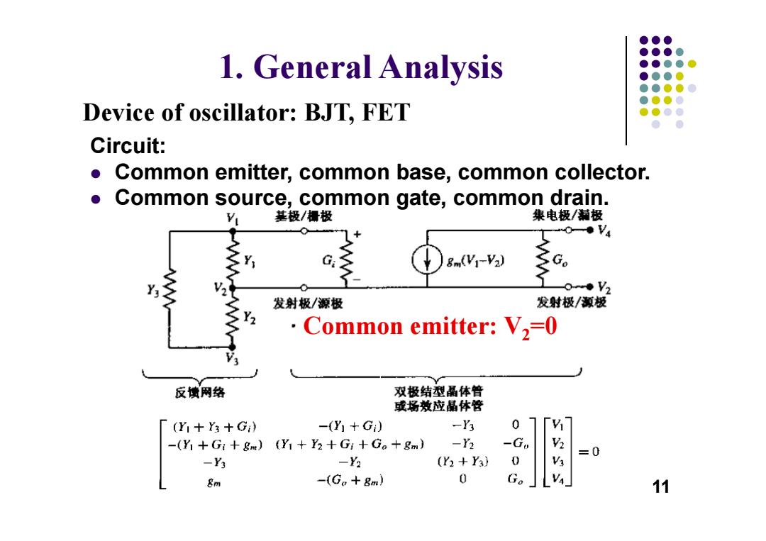
●●● ●●●● 1.General Analysis ●●●●● ●●●0 ●●●●0 ●●●0 Device of oscillator:BJT,FET ●●●● Circuit: Common emitter,common base,common collector. ● Common source,common gate,common drain. 基极/摄极 集电极/漏极 SY G 8m(Y-V2) 0◆V2 发射极/源极 发射极/源极 ·Common emitter:V2=0 反馈网络 双极结型晶体普 或场效应晶体管 「(Y1+Y3+G) -(Y十G) -Y3 0 7 -(Y1 +Gi+gm)(Y1+Y2+Gi+Go+8m) -Y2 -Go =0 -Y3 -Y2 (Y2+Y) 0 8m -(G。+gm) 0 Go 11Common emitter: V2=0 1. General Analysis Circuit: Common emitter, common base, common collector. Common source, common gate, common drain. Device of oscillator: BJT, FET 11