正在加载图片...
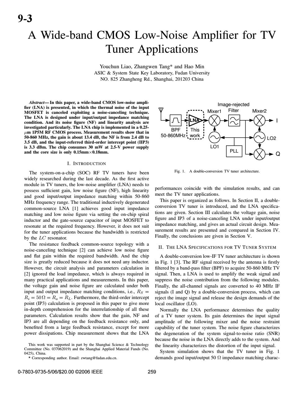
9-3 A Wide-band CMOS Low-Noise Amplifier for TV Tuner applications Youchun Liao,Zhangwen Tang*and Hao Min ASIC System State Key Laboratory,Fudan University NO.825 Zhangheng Rd.,Shanghai,201203 China Abstract-In this paper,a wide-band CMOS low-noise ampli- Image-rejected fier (LNA)is presented,in which the thermal noise of the input MOSFET is canceled exploiting a noise-canceling technique. Mixer1 Filter Mixer2 The LNA is designed under input/output impedance matching condition.And its noise figure (NF)and linearity analysis are investigated particularly.The LNA chip is implemented in a 0.25- BPF um 1P5M RF CMOS process.Measurement results show that in This 50-860 MHz,the gain is about 13.4 dB,the NF is from 2.4 dB to 50-860MHz work 02 3.5 dB,and the input-referred third-order intercept point (IIP3) is 3.3 dBm.The chip consumes 30 mW at 2.5-V power supply and the core size is only 0.15mmx0.18mm. PLL I.INTRODUCTION The system-on-a-chip (SOC)RF TV tuners have been Fig.1.A double-conversion TV tuner architecture. widely researched during the last decade.As the first active module in TV tuners,the low-noise amplifier (LNA)needs to possess sufficient gain,low noise figure (NF),high linearity performances coincide with the simulation results,and can and good input/output impedance matching within 50-860 meet the TV tuner applications. MHz frequency range.The traditional inductively degenerated This paper is organized as follows.In Section II,a double- common-source LNA [1]achieves good input impedance conversion TV tuner is introduced,and the LNA specifica- matching and low noise figure via setting the on-chip spiral tions are given.Section III calculates the voltage gain,noise inductor and the gate-source capacitor of input MOSFET to figure and IP3 of a noise-canceling LNA under input/output resonate at the required frequency.However,it does not suit impedance matching,and gives an actual circuit design.Mea- for the tuner applications because the bandwidth is restricted surement results are presented and compared in Section IV. by the LC resonator. Finally,the conclusions are given in Section V. The resistance feedback common-source topology with a II.THE LNA SPECIFICATIONS FOR TV TUNER SYSTEM noise-canceling technique [2]can achieve low noise figure and flat gain within the required bandwidth.And the chip A double-conversion low-IF TV tuner architecture is shown size is greatly reduced because it does not need any inductor.in Fig.1 [3].The RF signal received by the antenna is firstly However,the circuit analysis and parameters calculation in filtered by a band-pass filter(BPF)to acquire 50-860 MHz TV [2]ignored the load impedance,which is always required in signal.Then,a LNA is used to amplify the weak signal and many practical applications and measurements.In this paper,suppress the noise contribution from the following modules. the voltage gain and noise figure are calculated under both Finally,the all-channel signals are converted to 40 MHz IF input and output impedance matching conditions,i.e.,Rs= signals(I and Q)by a double-conversion process,which can R;=500=Ro=RL.Furthermore,the third-order intercept reject the image signal and release the design demands of the point(IP3)calculation is proposed in this paper to give more local oscillator (LO). in-depth comprehension for the interrelationship of all these Normally the LNA performance determines the quality parameters.Calculation results show that the gain,NF and of a TV tuner system.Its gain determines the input signal IP3 are all depending on the feedback resistance only,and amplitude of the following mixer and the noise restraint benefited from a large feedback resistance,except for more capability of the tuner system.The noise figure characterizes power dissipations.Chip measurement shows that the LNA the degeneration of the system signal-to-noise ratio (SNR) because the noise in the LNA directly adds to the system.And This work was supported in part by the Shanghai Science Technology the linearity characterizes the distortion of the input signal. Committee (No.037062019)and the Shanghai Applied Material Funds (No. 0425).China. System simulation shows that the TV tuner in Fig.1 Corresponding author.Email:zwtang@fudan.edu.cn. demands good input/output 50 impedance matching charac- 0-7803-9735-5/06/$20.00©20061EEE 259A Wide-band CMOS Low-Noise Amplifier for TV Tuner Applications Youchun Liao, Zhangwen Tang* and Hao Min ASIC & System State Key Laboratory, Fudan University NO. 825 Zhangheng Rd., Shanghai, 201203 China Abstract— In this paper, a wide-band CMOS low-noise ampli- fier (LNA) is presented, in which the thermal noise of the input MOSFET is canceled exploiting a noise-canceling technique. The LNA is designed under input/output impedance matching condition. And its noise figure (NF) and linearity analysis are investigated particularly. The LNA chip is implemented in a 0.25- µm 1P5M RF CMOS process. Measurement results show that in 50-860 MHz, the gain is about 13.4 dB, the NF is from 2.4 dB to 3.5 dB, and the input-referred third-order intercept point (IIP3) is 3.3 dBm. The chip consumes 30 mW at 2.5-V power supply and the core size is only 0.15mm×0.18mm. I. INTRODUCTION The system-on-a-chip (SOC) RF TV tuners have been widely researched during the last decade. As the first active module in TV tuners, the low-noise amplifier (LNA) needs to possess sufficient gain, low noise figure (NF), high linearity and good input/output impedance matching within 50-860 MHz frequency range. The traditional inductively degenerated common-source LNA [1] achieves good input impedance matching and low noise figure via setting the on-chip spiral inductor and the gate-source capacitor of input MOSFET to resonate at the required frequency. However, it does not suit for the tuner applications because the bandwidth is restricted by the LC resonator. The resistance feedback common-source topology with a noise-canceling technique [2] can achieve low noise figure and flat gain within the required bandwidth. And the chip size is greatly reduced because it does not need any inductor. However, the circuit analysis and parameters calculation in [2] ignored the load impedance, which is always required in many practical applications and measurements. In this paper, the voltage gain and noise figure are calculated under both input and output impedance matching conditions, i.e., RS = Ri = 50Ω = Ro = RL. Furthermore, the third-order intercept point (IP3) calculation is proposed in this paper to give more in-depth comprehension for the interrelationship of all these parameters. Calculation results show that the gain, NF and IP3 are all depending on the feedback resistance only, and benefited from a large feedback resistance, except for more power dissipations. Chip measurement shows that the LNA This work was supported in part by the Shanghai Science & Technology Committee (No. 037062019) and the Shanghai Applied Material Funds (No. 0425), China. * Corresponding author. Email: zwtang@fudan.edu.cn. PLL BPF LO1 LO2 Mixer1 Mixer2 Image-rejected Filter I Q This work LNA 50-860MHz Fig. 1. A double-conversion TV tuner architecture. performances coincide with the simulation results, and can meet the TV tuner applications. This paper is organized as follows. In Section II, a doubleconversion TV tuner is introduced, and the LNA specifications are given. Section III calculates the voltage gain, noise figure and IP3 of a noise-canceling LNA under input/output impedance matching, and gives an actual circuit design. Measurement results are presented and compared in Section IV. Finally, the conclusions are given in Section V. II. THE LNA SPECIFICATIONS FOR TV TUNER SYSTEM A double-conversion low-IF TV tuner architecture is shown in Fig. 1 [3]. The RF signal received by the antenna is firstly filtered by a band-pass filter (BPF) to acquire 50-860 MHz TV signal. Then, a LNA is used to amplify the weak signal and suppress the noise contribution from the following modules. Finally, the all-channel signals are converted to 40 MHz IF signals (I and Q) by a double-conversion process, which can reject the image signal and release the design demands of the local oscillator (LO). Normally the LNA performance determines the quality of a TV tuner system. Its gain determines the input signal amplitude of the following mixer and the noise restraint capability of the tuner system. The noise figure characterizes the degeneration of the system signal-to-noise ratio (SNR) because the noise in the LNA directly adds to the system. And the linearity characterizes the distortion of the input signal. System simulation shows that the TV tuner in Fig. 1 demands good input/output 50 Ω impedance matching charac- 0-7803-9735-5/06/$20.00 ©2006 IEEE 259 9-3