正在加载图片...
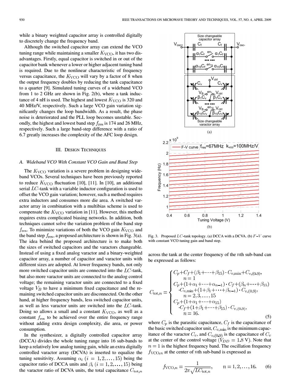
930 IEEE TRANSACTIONS ON MICROWAVE THEORY AND TECHNIQUES.VOL.57.NO.4.APRIL 2009 while a binary weighted capacitor array is controlled digitally Size changeable to discretely change the frequency band. capacitor array Although the switched capacitor array can extend the VCO Cr tuning range while maintaining a smaller KvCo,it has two dis- en a1Cf advantages.Firstly,equal capacitor is switched in or out of the capacitor bank whenever a lower or higher adjacent tuning band a1sC is required.Due to the nonlinear characteristic of frequency versus capacitance,the Kvco will vary by a factor of 8 when the output frequency doubles by reducing the tank capacitance to a quarter [9].Simulated tuning curves of a wideband VCO from 1 to 2 GHz are shown in Fig.2(b),where a tank induc- tance of 4 nH is used.The highest and lowest Kvco is 320 and 40 MHz/V,respectively.Such a large VCO gain variation sig- nificantly changes the loop bandwidth.As a result,the phase noise is deteriorated and the PLL loop becomes unstable.Sec- ondly,the highest and lowest band step fres is 174 and 26 MHz, Size changeable varactor array respectively.Such a large band-step difference with a ratio of (a) 6.7 greatly increases the complexity of the AFC loop design. 2.2*109 -F-V curve fres=67MHz Kvco=100MHz/V III.DESIGN TECHNIQUES A.Wideband VCO With Constant VCO Gain and Band Step 1.8 The Kvco variation is a severe problem in designing wide- band VCOs.Several techniques have been previously reported to reduce Kvco fluctuation [10].[11].In [10],an additional anba serial LC-tank with a variable inductor configuration is used to offset the VCO gain variation;however,such a method requires extra inductors and consumes more die area.A switched var- actor array in combination with a multibias scheme is used to compensate the Kvco variation in [11].However,this method requires extra complicated biasing networks.In addition,both 0.4 0.6 0.8 1 1.2 1.4 Tuning Voltage (V) techniques cannot solve the variation problem of the band step fres.To minimize variations of both the VCO gain Kyco and (b) the band step fres,a proposed architecture is shown in Fig.3(a). Fig.3.Proposed LC-tank topology.(a)DCCA with a DCVA.(b)F-V curve The idea behind the proposed architecture is to make both with constant VCO tuning gain and band step. the sizes of switched capacitors and the varactors changeable. Instead of using a fixed analog varactor and a binary-weighted across the tank at the center frequency of the nth sub-band can capacitor array,a number of capacitor and varactor units with be expressed as follows: different sizes are adopted.At lower frequency bands,not only more switched capacitor units are connected into the LC-tank, Cp+Cf+(3+…+35)Cw,min+C,0.9, but also more varactor units are connected to the analog control m=1 voltage;the remaining varactor units are connected to a fixed Cp+(1+1+…+anm-1)Cf+(3n+…+35) voltage VB to have a minimum fixed capacitance and the re- Cu,mim+(1++…+3n-1)C,(0.9y maining switched capacitor units are disconnected.On the other Ctot,n n=2,3,,15 hand,at higher frequency bands,less switched capacitor units, Cp+(1+a1+…+15) as well as less varactor units are switched into the LC-tank. .Cf+(1+31+…+315)Cu,0.9): Doing so allows a small and a constant Kvco,as well as a m=16. constant fres to be achieved over the entire frequency range (5) without adding extra design complexity,die area,or power where Cp is the parasitic capacitance,Cf is the capacitance of consumption. the basic switched capacitor unit.Cv,min is the minimum capac- In the synthesizer,a digitally controlled capacitor array itance of the varactor C,and C,(0)is the capacitance of C (DCCA)divides the whole tuning range into 16 sub-bands to at the center of the control voltage(VDD=1.8 V).Note that keep a relatively low analog tuning gain,while an extra digitally n=1 is the highest frequency band.The oscillation frequency controlled varactor array (DCVA)is inserted to equalize the fvco,n at the center of nth sub-band is expressed as tuning sensitivity.Assuming ai(=1,2,...,15)being the capacitor ratio of DCCA units and Bi(=1,2,...,15)being 1 (6) the varactor ratio of DCVA units,the total capacitance Ctot,n fco,n=2m√Ctot,n n=1,2,.…,16.930 IEEE TRANSACTIONS ON MICROWAVE THEORY AND TECHNIQUES, VOL. 57, NO. 4, APRIL 2009 while a binary weighted capacitor array is controlled digitally to discretely change the frequency band. Although the switched capacitor array can extend the VCO tuning range while maintaining a smaller , it has two disadvantages. Firstly, equal capacitor is switched in or out of the capacitor bank whenever a lower or higher adjacent tuning band is required. Due to the nonlinear characteristic of frequency versus capacitance, the will vary by a factor of 8 when the output frequency doubles by reducing the tank capacitance to a quarter [9]. Simulated tuning curves of a wideband VCO from 1 to 2 GHz are shown in Fig. 2(b), where a tank inductance of 4 nH is used. The highest and lowest is 320 and 40 MHz/V, respectively. Such a large VCO gain variation significantly changes the loop bandwidth. As a result, the phase noise is deteriorated and the PLL loop becomes unstable. Secondly, the highest and lowest band step is 174 and 26 MHz, respectively. Such a large band-step difference with a ratio of 6.7 greatly increases the complexity of the AFC loop design. III. DESIGN TECHNIQUES A. Wideband VCO With Constant VCO Gain and Band Step The variation is a severe problem in designing wideband VCOs. Several techniques have been previously reported to reduce fluctuation [10], [11]. In [10], an additional serial -tank with a variable inductor configuration is used to offset the VCO gain variation; however, such a method requires extra inductors and consumes more die area. A switched varactor array in combination with a multibias scheme is used to compensate the variation in [11]. However, this method requires extra complicated biasing networks. In addition, both techniques cannot solve the variation problem of the band step . To minimize variations of both the VCO gain and the band step , a proposed architecture is shown in Fig. 3(a). The idea behind the proposed architecture is to make both the sizes of switched capacitors and the varactors changeable. Instead of using a fixed analog varactor and a binary-weighted capacitor array, a number of capacitor and varactor units with different sizes are adopted. At lower frequency bands, not only more switched capacitor units are connected into the -tank, but also more varactor units are connected to the analog control voltage; the remaining varactor units are connected to a fixed voltage to have a minimum fixed capacitance and the remaining switched capacitor units are disconnected. On the other hand, at higher frequency bands, less switched capacitor units, as well as less varactor units are switched into the -tank. Doing so allows a small and a constant , as well as a constant to be achieved over the entire frequency range without adding extra design complexity, die area, or power consumption. In the synthesizer, a digitally controlled capacitor array (DCCA) divides the whole tuning range into 16 sub-bands to keep a relatively low analog tuning gain, while an extra digitally controlled varactor array (DCVA) is inserted to equalize the tuning sensitivity. Assuming being the capacitor ratio of DCCA units and being the varactor ratio of DCVA units, the total capacitance Fig. 3. Proposed -tank topology. (a) DCCA with a DCVA. (b) – curve with constant VCO tuning gain and band step. across the tank at the center frequency of the th sub-band can be expressed as follows: (5) where is the parasitic capacitance, is the capacitance of the basic switched capacitor unit, is the minimum capacitance of the varactor , and is the capacitance of at the center of the control voltage V . Note that is the highest frequency band. The oscillation frequency at the center of th sub-band is expressed as (6)��