正在加载图片...
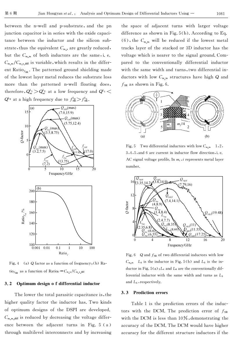
第6期 Jian Hongyan et al.Analysis and Optimum Design of Differential Inductors Using... 1081 between the n-well and p-substrate,and the pn the space of adjacent turns with larger voltage junction capacitor is in series with the oxide capaci- difference as shown in Fig.5(b).According to Eq. tance between the inductor and the silicon sub- (6),the Cm will be reduced if the lowest metal strate,thus the equivalent Cm are greatly reduced, tracks layer of the stacked or 3D inductor has the but the Cmm of both inductors are the same,i.e. voltage which is nearer to the signal ground.Com- Cmm/Cmd is variable,which results in the differ- pared to the conventionally differential inductor ent Ratio The patterned ground shielding made with the same width and turns,two differential in- of the lowest layer metal reduces the substrate loss ductors with low Cmm structures have high Q and more than the patterned n-well floating does, fsk as shown in Fig.6. therefore,Q>Q at a low frequency and Q< Q':at a high frequency due to fs>fsk. (a) O.(max) 15 (7.0.15.9) Qdn(max) (5.75,12.4 10 m/4 (max) 3.5.8.75) (a) (b) Q,.{max) Fig.5 Two differential inductors with low Cmm 1,2. (3.2.7.5) 138入17.0) 3.4.5.and 6 are current in inductor flow direction.i.e. (72) 13.75) AC signal voltage profile.In m,,i represents metal layer number. 10 Frequency/GHz O. 16335.14.2314 7.79.16) (b) 200 12 180H (7.4.14.1) (4,8.9 160 9i19.48 140 (2.4,7.7) 2.35,6.8 2(8.35 9I1) :869 Pwn(11.55入 1204 :(6.6 Q(655 017.25 0 8 12 20 10 Frequency/GHz 0.0010.010.1110100 Ratio Fig.6 Q and fsg of two differential inductors with low Fig.4 (a)Q factor as a function of fregnency;(b)Ra- Cmm La is the inductor in Fig.5(b)and Ls is the in- ductor in Fig.5(a);L and Ls are the conventionally dif- tio/sg as a function of Ratioc=C/Cm ferential inductor with the same width and turns as La 3.2 Optimum design o f differential inductor and L,respectively. The lower the total parasitic capacitance is,the 3.3 Prediction errors higher quality factor the inductor has.Two kinds Table 1 is the prediction errors of the induc- of optimum designs of the DSPI are developed. tors with the DCM.The prediction error of fs& C is reduced by decreasing the voltage differ- with the DCM is less than 10%,demonstrating the ence between the adjacent turns in Fig.5(a) accuracy of the DCM.The DCM would have higher through multilevel interconnects and by increasing accuracy for the different structure inductors if the第0期 I567Q97L367)J/>S! U76@325267C+?45;G;B>25L79AB5AA>F>7456@!7CG:49F2V257L" H>4=>>748>7&=>@@67C ?&2GH24F64>#67C48>?7 TG7:4597:6?6:549F52572>F5>2=54848>9R5C>:6?6:5& 467:>H>4=>>748>57CG:49F67C48>25@5:972GH& 24F64>#48G248>>XG5\6@>74.;26F>LF>64@3F>CG:>C# HG448>.; ; 9AH94857CG:49F26F>48>26;>#5,>, .; ;$.;2C5AA52\6F56H@>#=85:8F>2G@425748>C5AA>F& >74Z6459D"Z ,<8>?644>F7>CLF9G7C285>@C57L;6C> 9A48>@9=>24@63>F;>46@F>CG:>248>2GH24F64>@922 ;9F>4867 48> ?644>F7>C 7&=>@@A@96457L C9>2# 48>F>A9F>#?-) 2> )?-- 2> 646@9=AF>XG>7:367C?-) * ?-- 64685L8AF>XG>7:3CG>49D-- "Z)D-) "Z, D5L,* %6&?A6:49F626AG7:45979AAF>L7>7:3’%H&Z6& 459D"Z 626AG7:45979AZ6459. b.; 7$.; 2C5AA T[+ %C>IP;PK=@IX<8LKILL=?=<>IB9I<K;M>8? <8>@9=>F48>4946@?6F62545::6?6:5467:>52#48> 85L8>FXG6@543A6:49F48>57CG:49F862,<=9_57C2 9A9?45;G; C>25L729A48> B"[!6F>C>\>@9?>C, .; ; C5AA52F>CG:>CH3C>:F>6257L48>\9@46L>C5AA>F& >7:>H>4=>>7 48> 6CT6:>744GF7257 D5L,/%6& 48F9GL8;G@45@>\>@574>F:977>:4267CH357:F>6257L 48>2?6:> 9A6CT6:>744GF72 =548@6FL>F \9@46L> C5AA>F>7:>62289=757D5L,/%H&,U::9FC57L49JX, %00>.; ; =5@@H>F>CG:>C5A48>@9=>24;>46@ 4F6:_2@63>F9A48>246:_>C9F(B57CG:49F86248> \9@46L>=85:8527>6F>F4948>25L76@LF9G7C,O9;& ?6F>C4948>:97\>745976@@3 C5AA>F>7456@57CG:49F =54848>26;>=5C4867C4GF72#4=9C5AA>F>7456@57& CG:49F2=548@9=.; ; 24FG:4GF>286\>85L8?67C D"Z62289=757D5L,0, D5L,/ <=9C5AA>F>7456@57CG:49F2=548@9=.; ; )#-# (#*#/#67C06F>:GFF>745757CG:49FA@9=C5F>:4597#5,>, UO25L76@\9@46L>?F9A5@>,!7C%#%F>?F>2>742;>46@@63>F 7G;H>F, D5L,0 ?67CD"Z9A4=9C5AA>F>7456@57CG:49F2=548@9= .; ; -(5248>57CG:49F57D5L,/%H&67C-/5248>57& CG:49F57D5L,/%6&’-*67C-06F>48>:97\>745976@@3C5A& A>F>7456@57CG:49F=54848>26;>=5C4867C4GF7262-( 67C-/#F>2?>:45\>@3, T:T A?=KIM>I8<=??8?@ <6H@>)5248>?F>C5:4597>FF9F29A48>57CG:& 49F2 =54848> BOW,<8>?F>C5:4597>FF9F9AD"Z =54848>BOW52@>224867)’d#C>;9724F6457L48> 6::GF6:39A48>BOW,<8>BOW =9G@C86\>85L8>F 6::GF6:3A9F48>C5AA>F>7424FG:4GF>57CG:49F25A48> )’1)