正在加载图片...
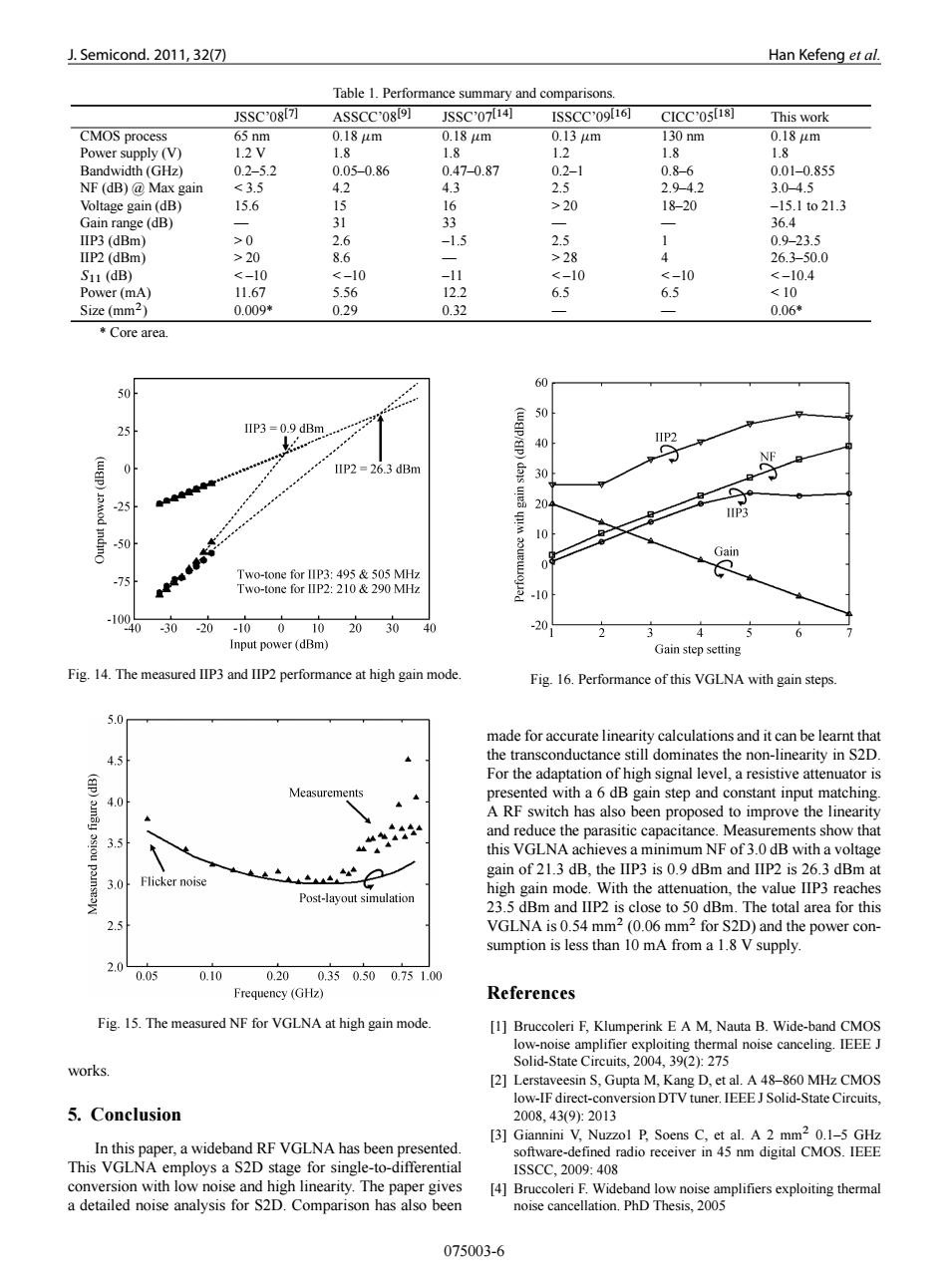
.Semicond..2011,32(7) Han Kefeng et al. Table 1.Performance summary and comparisons. JSSC08l可 ASSCC'08[9] JSSC'0714 ISSCC'09l1可 CICC'05[18] This work CMOS process 65 nm 0.18um 0.18um 0.13um 130nm 0.18um Power supply (V) 1.2V 1.8 1.8 1.2 1.8 1.8 Bandwidth(GHz) 0.2-5.2 0.05-0.86 0.47-0.87 0.2-1 0.8-6 0.01-0.855 NF (dB)@Max gain <3.5 4.2 4.3 2.5 2.9-4.2 3.0-4.5 Voltage gain(dB) 15.6 16 >20 18-20 -15.1to21.3 Gain range(dB) 31 33 36.4 IIP3 (dBm) >0 2.6 -1.5 2.5 1 0.9-23.5 IIP2 (dBm) >20 8.6 >28 26.3-50.0 S11(dB) <-10 <-10 -11 <-10 <-10 <-10.4 Power(mA) 11.67 5.56 12.2 6.5 6.5 <10 Size(mm2) 0.009* 0.29 0.32 0.06* Core area * 50 50 25 IIP3 =0.9 dBm (wgP/gP) 40 0 IIP2 26.3 dBm -25 20 -50 Gain 75 Two-tone for IIP3:495 505 MHz Two-tone for IIP2:210&290 MHz -10 40-30 -20-100102030 40 -20 3 4 Input power (dBm) Gain step setting Fig.14.The measured IIP3 and IIP2 performance at high gain mode. Fig.16.Performance of this VGLNA with gain steps. 5.0 made for accurate linearity calculations and it can be learnt that 4.5 the transconductance still dominates the non-linearity in S2D (P For the adaptation of high signal level,a resistive attenuator is Measurements 4.0 presented with a 6 dB gain step and constant input matching. A RF switch has also been proposed to improve the linearity and reduce the parasitic capacitance.Measurements show that SIOU 3.5 this VGLNA achieves a minimum NF of 3.0 dB with a voltage gain of 21.3 dB,the IIP3 is 0.9 dBm and IIP2 is 26.3 dBm at 3.0 Flicker noise 心心 high gain mode.With the attenuation,the value IIP3 reaches Post-layout simulation 23.5 dBm and IIP2 is close to 50 dBm.The total area for this 2.5 VGLNA is 0.54 mm2(0.06 mm2 for S2D)and the power con- sumption is less than 10 mA from a 1.8 V supply. 2.0 0.05 0.10 0.200.350.500.751.00 Frequency (GHz) References Fig.15.The measured NF for VGLNA at high gain mode. [1]Bruccoleri F,Klumperink E A M,Nauta B.Wide-band CMOS low-noise amplifier exploiting thermal noise canceling.IEEE J works. Solid-State Circuits,2004,39(2):275 [2]Lerstaveesin S,Gupta M,Kang D,et al.A 48-860 MHz CMOS low-IF direct-conversion DTV tuner.IEEE J Solid-State Circuits. 5.Conclusion 2008.43(9):2013 [3]Giannini V,Nuzzol P.Soens C,et al.A 2 mm2 0.1-5 GHz In this paper,a wideband RF VGLNA has been presented. software-defined radio receiver in 45 nm digital CMOS.IEEE This VGLNA employs a S2D stage for single-to-differential ISSCO,2009:408 conversion with low noise and high linearity.The paper gives [4]Bruccoleri F.Wideband low noise amplifiers exploiting thermal a detailed noise analysis for S2D.Comparison has also been noise cancellation.PhD Thesis,2005 075003-6J. Semicond. 2011, 32(7) Han Kefeng et al. Table 1. Performance summary and comparisons. JSSC’08Œ7 ASSCC’08Œ9 JSSC’07Œ14 ISSCC’09Œ16 CICC’05Œ18 This work CMOS process 65 nm 0.18 m 0.18 m 0.13 m 130 nm 0.18 m Power supply (V) 1.2 V 1.8 1.8 1.2 1.8 1.8 Bandwidth (GHz) 0.2–5.2 0.05–0.86 0.47–0.87 0.2–1 0.8–6 0.01–0.855 NF (dB) @ Max gain < 3.5 4.2 4.3 2.5 2.9–4.2 3.0–4.5 Voltage gain (dB) 15.6 15 16 > 20 18–20 –15.1 to 21.3 Gain range (dB) — 31 33 — — 36.4 IIP3 (dBm) > 0 2.6 –1.5 2.5 1 0.9–23.5 IIP2 (dBm) > 20 8.6 — > 28 4 26.3–50.0 S11 (dB) < –10 < –10 –11 < –10 < –10 < –10.4 Power (mA) 11.67 5.56 12.2 6.5 6.5 < 10 Size (mm2 ) 0.009* 0.29 0.32 — — 0.06* * Core area. Fig. 14. The measured IIP3 and IIP2 performance at high gain mode. Fig. 15. The measured NF for VGLNA at high gain mode. works. 5. Conclusion In this paper, a wideband RF VGLNA has been presented. This VGLNA employs a S2D stage for single-to-differential conversion with low noise and high linearity. The paper gives a detailed noise analysis for S2D. Comparison has also been Fig. 16. Performance of this VGLNA with gain steps. made for accurate linearity calculations and it can be learnt that the transconductance still dominates the non-linearity in S2D. For the adaptation of high signal level, a resistive attenuator is presented with a 6 dB gain step and constant input matching. A RF switch has also been proposed to improve the linearity and reduce the parasitic capacitance. Measurements show that this VGLNA achieves a minimum NF of 3.0 dB with a voltage gain of 21.3 dB, the IIP3 is 0.9 dBm and IIP2 is 26.3 dBm at high gain mode. With the attenuation, the value IIP3 reaches 23.5 dBm and IIP2 is close to 50 dBm. The total area for this VGLNA is 0.54 mm2 (0.06 mm2 for S2D) and the power consumption is less than 10 mA from a 1.8 V supply. References [1] Bruccoleri F, Klumperink E A M, Nauta B. Wide-band CMOS low-noise amplifier exploiting thermal noise canceling. IEEE J Solid-State Circuits, 2004, 39(2): 275 [2] Lerstaveesin S, Gupta M, Kang D, et al. A 48–860 MHz CMOS low-IF direct-conversion DTV tuner. IEEE J Solid-State Circuits, 2008, 43(9): 2013 [3] Giannini V, Nuzzo1 P, Soens C, et al. A 2 mm2 0.1–5 GHz software-defined radio receiver in 45 nm digital CMOS. IEEE ISSCC, 2009: 408 [4] Bruccoleri F. Wideband low noise amplifiers exploiting thermal noise cancellation. PhD Thesis, 2005 075003-6