正在加载图片...
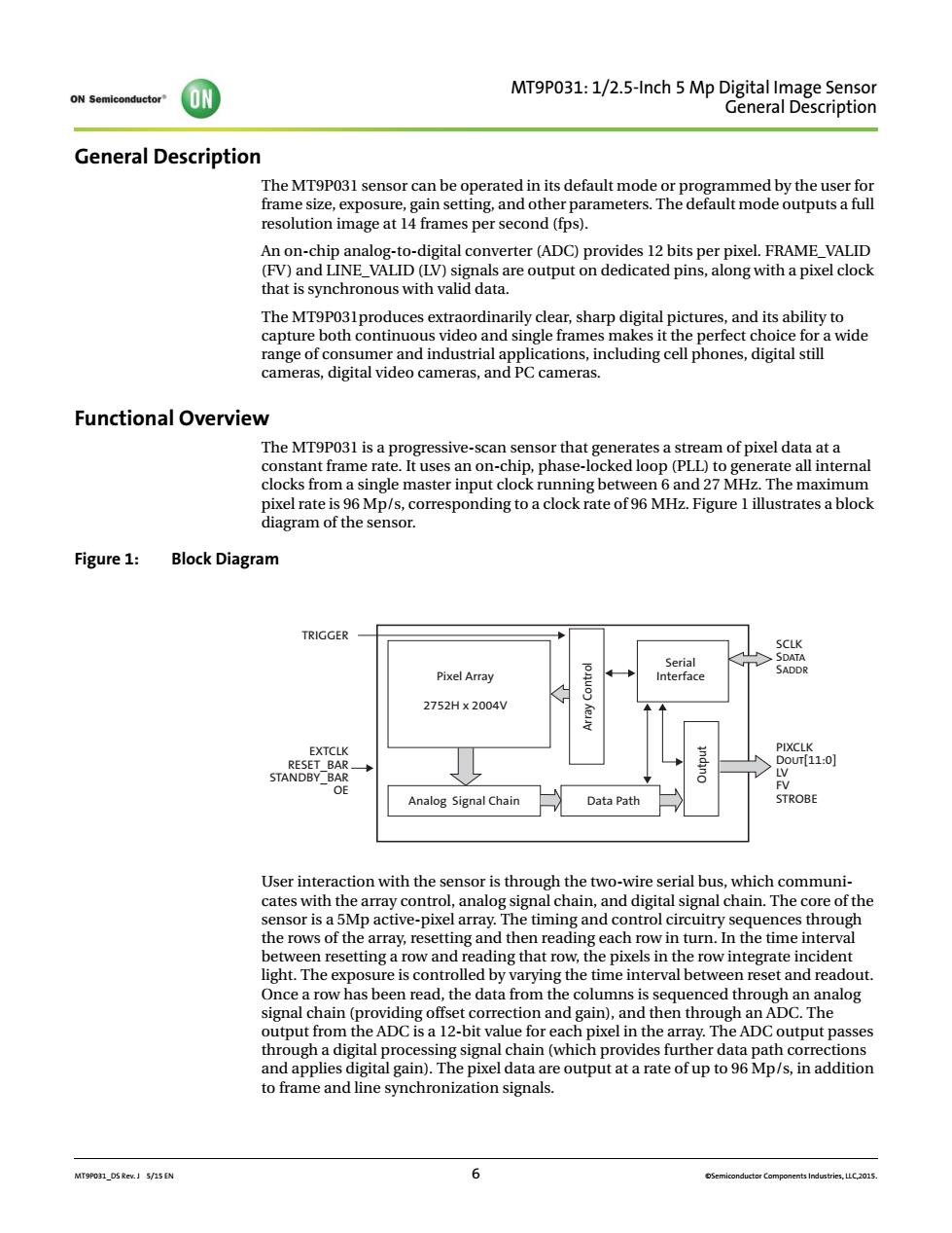
ON /2-InchMp General Description An on-chip analog-to-digital converter (ADC)provides 12 bits per pixel.FRAME_VALID The MT9P031produces extraordinarily clear,sharp digital pictures,and its ability to cameras Functional Overview l clocks from a single master input clock running between 6 and 27 MHz The maximum pixel rate is96 Mp/s,corresponding to a clock rate of96 MHz.Figure 1 illustrates a block diagram of the sensor. Figure 1:Block Diagram GGER Pixel Array nierl 2752H×2004V 网 Analog Signal Chain Data Path STRORE User interaction with the sensor is through the two-wire serial bus,which communi- cates with the array control,analog signal chain,and digital signal chain.The core of the sensor isa 5Mp active-pixel array.The tming e incident light.The exposure is controlled by varying the time interval between reset and readout. que 1-au)and th nced through an analog hen through a AD through a digital processing signal chain (which provides further data path corre and applies digital gain).The pixel data are output at a rate ofup toMp/s,in addition to frame and line synchronization signals. MT3P_0cs/N 6 MT9P031_DS Rev. J 5/15 EN 6 ©Semiconductor Components Industries, LLC,2015. MT9P031: 1/2.5-Inch 5 Mp Digital Image Sensor General Description General Description The MT9P031 sensor can be operated in its default mode or programmed by the user for frame size, exposure, gain setting, and other parameters. The default mode outputs a full resolution image at 14 frames per second (fps). An on-chip analog-to-digital converter (ADC) provides 12 bits per pixel. FRAME_VALID (FV) and LINE_VALID (LV) signals are output on dedicated pins, along with a pixel clock that is synchronous with valid data. The MT9P031produces extraordinarily clear, sharp digital pictures, and its ability to capture both continuous video and single frames makes it the perfect choice for a wide range of consumer and industrial applications, including cell phones, digital still cameras, digital video cameras, and PC cameras. Functional Overview The MT9P031 is a progressive-scan sensor that generates a stream of pixel data at a constant frame rate. It uses an on-chip, phase-locked loop (PLL) to generate all internal clocks from a single master input clock running between 6 and 27 MHz. The maximum pixel rate is 96 Mp/s, corresponding to a clock rate of 96 MHz. Figure 1 illustrates a block diagram of the sensor. Figure 1: Block Diagram User interaction with the sensor is through the two-wire serial bus, which communicates with the array control, analog signal chain, and digital signal chain. The core of the sensor is a 5Mp active-pixel array. The timing and control circuitry sequences through the rows of the array, resetting and then reading each row in turn. In the time interval between resetting a row and reading that row, the pixels in the row integrate incident light. The exposure is controlled by varying the time interval between reset and readout. Once a row has been read, the data from the columns is sequenced through an analog signal chain (providing offset correction and gain), and then through an ADC. The output from the ADC is a 12-bit value for each pixel in the array. The ADC output passes through a digital processing signal chain (which provides further data path corrections and applies digital gain). The pixel data are output at a rate of up to 96 Mp/s, in addition to frame and line synchronization signals. Pixel Array 2752H x 2004V SCLK SDATA SADDR PIXCLK DOUT[11:0] LV FV STROBE Serial Interface Analog Signal Chain Data Path TRIGGER EXTCLK RESET_BAR STANDBY_BAR OE Array Control Output