正在加载图片...
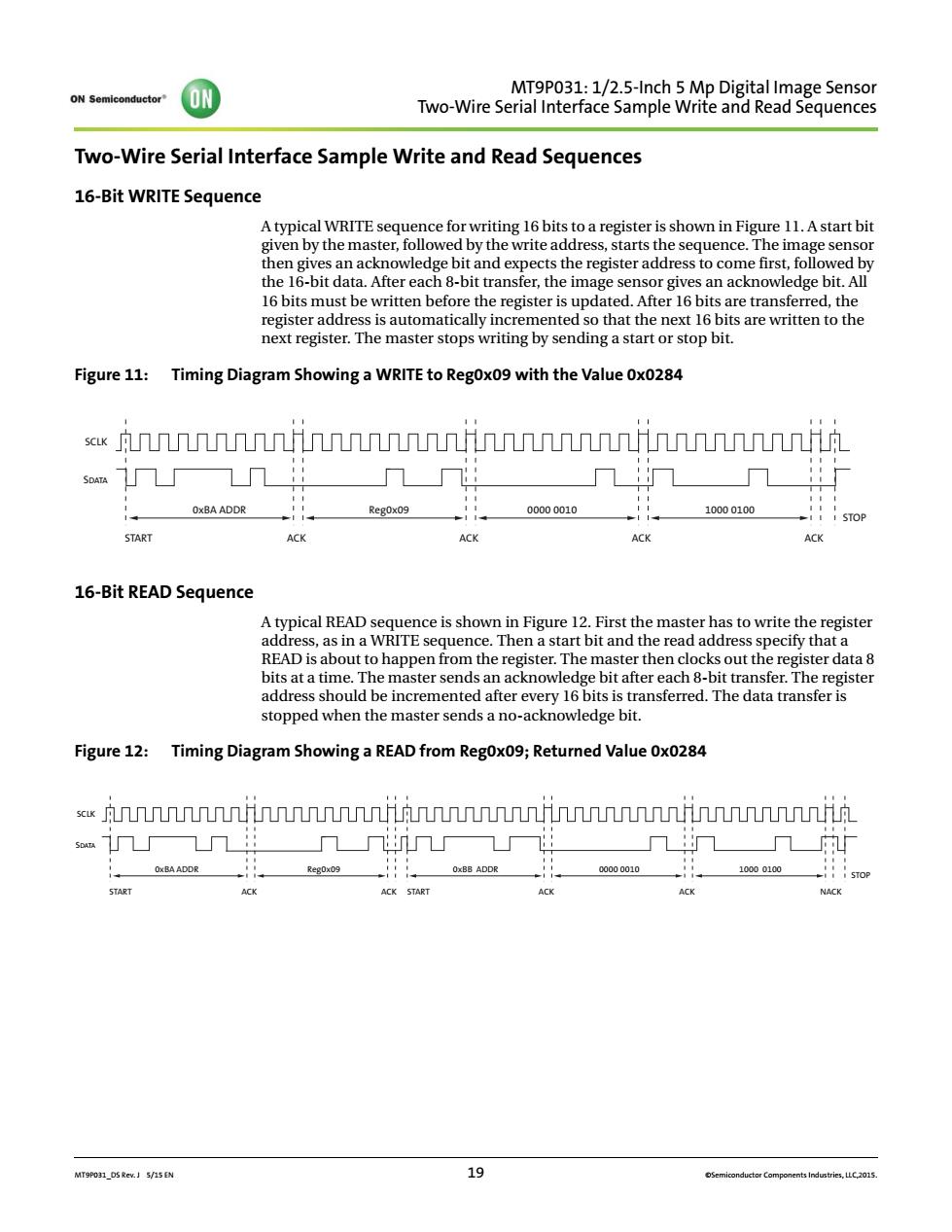
ON equen Two-Wire Serial Interface Sample Write and Read Sequences 16-Bit WRITE Sequence typicalwbtshownne1.Astarb given by th the 16-bit data.After each 8-bit transfer,the image sensor gives an acknowledge bit All 16 bits mus st be written before the register is updated.After 16 bits are transferred,the register a o that the next le s are written to the ext register ending a start or stop bit. Figure 11:Timing Diagram Showing a WRITE to Regox09 with the Value 0x0284 annnnnnnniinnnnnnnniinnnnnnnniinnnnnnnniir sw几 OxBAADDR 00000010 10000100 START ACK 16-Bit READ Sequence READ is about to happen from the register.The master then clocks out the register data The master sends an acknowled addres alter every I ts is transferred.The data transfer is stopped when the master sends a no-acknowledge bi Figure 12:Timing Diagram Showing a READ from RegOx09;Returned Value 0x0284 Annnnnnnninnnnnnnnfannnnnnnniinnnnnnnniinnnnnnnni m17几几 几几 几 000001011 1000010 OK START 9MT9P031_DS Rev. J 5/15 EN 19 ©Semiconductor Components Industries, LLC,2015. MT9P031: 1/2.5-Inch 5 Mp Digital Image Sensor Two-Wire Serial Interface Sample Write and Read Sequences Two-Wire Serial Interface Sample Write and Read Sequences 16-Bit WRITE Sequence A typical WRITE sequence for writing 16 bits to a register is shown in Figure 11. A start bit given by the master, followed by the write address, starts the sequence. The image sensor then gives an acknowledge bit and expects the register address to come first, followed by the 16-bit data. After each 8-bit transfer, the image sensor gives an acknowledge bit. All 16 bits must be written before the register is updated. After 16 bits are transferred, the register address is automatically incremented so that the next 16 bits are written to the next register. The master stops writing by sending a start or stop bit. Figure 11: Timing Diagram Showing a WRITE to Reg0x09 with the Value 0x0284 16-Bit READ Sequence A typical READ sequence is shown in Figure 12. First the master has to write the register address, as in a WRITE sequence. Then a start bit and the read address specify that a READ is about to happen from the register. The master then clocks out the register data 8 bits at a time. The master sends an acknowledge bit after each 8-bit transfer. The register address should be incremented after every 16 bits is transferred. The data transfer is stopped when the master sends a no-acknowledge bit. Figure 12: Timing Diagram Showing a READ from Reg0x09; Returned Value 0x0284 SCLK SDATA START ACK 0xBA ADDR ACK ACK ACK STOP Reg0x09 0000 0010 1000 0100 SCLK SDATA START ACK 0xBA ADDR 0xBB ADDR 0000 0010 Reg0x09 ACK ACK ACK STOP 1000 0100 START NACK