正在加载图片...
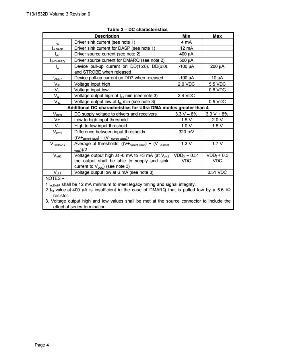
T13/1532D Volume 3 Revision 0 Table 2-DC characteristics Description Min Max Driver sink current(see note 1) 4mA IoLDASP Driver sink current for DASP(see note 1) 12 mA loH Driver source current(see note 2) 400A oHDMARQ Driver source current for DMARQ(see note 2) 500A 2 Device pull-up current on DD(15:8),DD(6:0). -100A 200A and STROBE when released lZDD7 Device pull-up current on DD7 when released -100A 10A ViH Voltage input high 2.0 VDC 5.5 VDC iL Voltage input low 0.8VDC V Voltage output high at l min(see note 3) 2.4 VDC V Voltage output low at l min (see note 3) 0.5 VDC Additional DC characteristics for Ultra DMA modes greater than 4 Vpp3 DC supply voltage to drivers and receivers 3.3V-8% 3.3V+8% V+ Low to high input threshold 1.5V 2.0V V- High to low input threshold 1.0V 1.5V VHYS Difference between input thresholds: 320mV (V+cmrent value)-(V-curent vatue)) VTHRAVG Average of thresholds:((V+cument value)+V-cumen 1.3V 1.7V ae)/2 VoH2 Voltage output high at-6 mA to +3 mA(at VoH2 VDD3-0.51 VDD3+0.3 the output shall be able to supply and sink VDC VDC current to VDDa)(see note 3) Va2 Voltage output low at 6 mA(see note 3) 0.51 VDC NOTES- 1 lLDAsP shall be 12 mA minimum to meet legacy timing and signal integrity. 2 value at 400 uA is insufficient in the case of DMARQ that is pulled low by a 5.6K resistor. 3.Voltage output high and low values shall be met at the source connector to include the effect of series termination. Page 4T13/1532D Volume 3 Revision 0 Page 4 Table 2 − DC characteristics Description Min Max IoL Driver sink current (see note 1) 4 mA IoLDASP Driver sink current for DASP (see note 1) 12 mA IoH Driver source current (see note 2) 400 µA IoHDMARQ Driver source current for DMARQ (see note 2) 500 µA IZ Device pull-up current on DD(15:8), DD(6:0), and STROBE when released -100 µA 200 µA IZDD7 Device pull-up current on DD7 when released -100 µA 10 µA ViH Voltage input high 2.0 VDC 5.5 VDC ViL Voltage input low 0.8 VDC VoH Voltage output high at IoH min (see note 3) 2.4 VDC VoL Voltage output low at IoL min (see note 3) 0.5 VDC Additional DC characteristics for Ultra DMA modes greater than 4 VDD3 DC supply voltage to drivers and receivers 3.3 V – 8% 3.3 V + 8% V+ Low to high input threshold 1.5 V 2.0 V V− High to low input threshold 1.0 V 1.5 V VHYS Difference between input thresholds: ((V+current value) − (V−current value)) 320 mV VTHRAVG Average of thresholds: ((V+current value) + (V−current value))/2 1.3 V 1.7 V VoH2 Voltage output high at -6 mA to +3 mA (at VoH2 the output shall be able to supply and sink current to VDD3) (see note 3) VDD3 – 0.51 VDC VDD3 + 0.3 VDC VoL2 Voltage output low at 6 mA (see note 3) 0.51 VDC NOTES − 1 IoLDASP shall be 12 mA minimum to meet legacy timing and signal integrity. 2 IoH value at 400 µA is insufficient in the case of DMARQ that is pulled low by a 5.6 kΩ resistor. 3. Voltage output high and low values shall be met at the source connector to include the effect of series termination