正在加载图片...
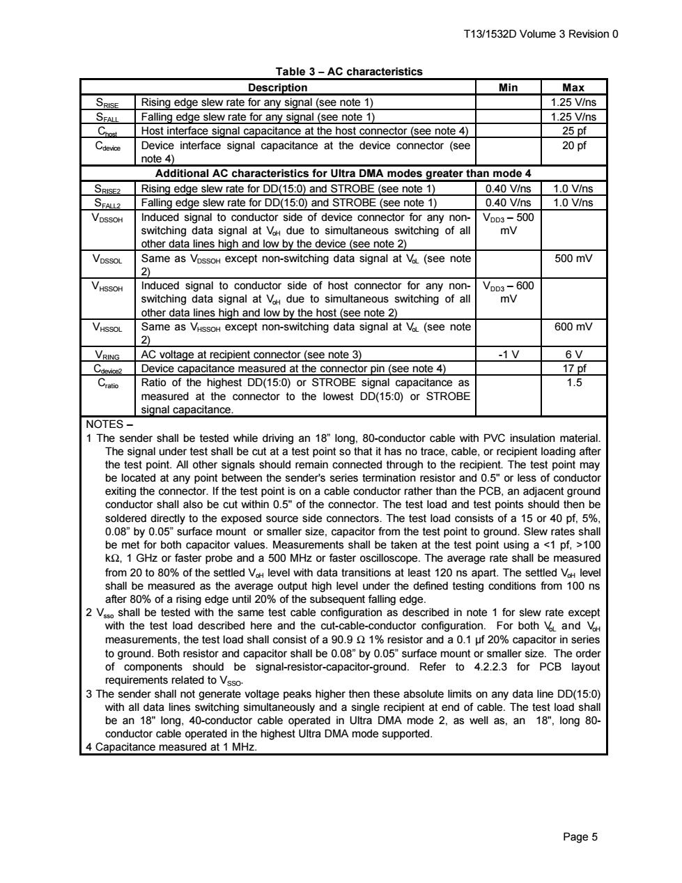
T13/1532D Volume 3 Revision 0 Table 3-AC characteristics Description Min Max SRISE Rising edge slew rate for any signal(see note 1) 1.25 V/ns SFALL Falling edge slew rate for any signal(see note 1) 1.25 V/ns Chost Host interface signal capacitance at the host connector(see note 4) 25 pf Cdevice Device interface signal capacitance at the device connector (see 20pf note 4) Additional AC characteristics for Ultra DMA modes greater than mode 4 SRISE2 Rising edge slew rate for DD(15:0)and STROBE (see note 1) 0.40 V/ns 1.0 V/ns SFALL2 Falling edge slew rate for DD(15:0)and STROBE (see note 1) 0.40 V/ns 1.0 V/ns VDSSoH Induced signal to conductor side of device connector for any non- VoD3-500 switching data signal at Vh due to simultaneous switching of all mV other data lines high and low by the device (see note 2) VpssoL Same as VossoH except non-switching data signal at VL (see note 500mV 2) VHSSOH Induced signal to conductor side of host connector for any non- V0o3-600 switching data signal at V due to simultaneous switching of all mV other data lines high and low by the host(see note 2) VHSSOL Same as VHssoH except non-switching data signal at VaL (see note 600mV 2 VRING AC voltage at recipient connector(see note 3) -1V 6V Cdevice2 Device capacitance measured at the connector pin(see note 4) 17 pf Cratio Ratio of the highest DD(15:0)or STROBE signal capacitance as 1.5 measured at the connector to the lowest DD(15:0)or STROBE signal capacitance. NOTES- 1 The sender shall be tested while driving an 18"long,80-conductor cable with PVC insulation material. The signal under test shall be cut at a test point so that it has no trace,cable,or recipient loading after the test point.All other signals should remain connected through to the recipient.The test point may be located at any point between the sender's series termination resistor and 0.5"or less of conductor exiting the connector.If the test point is on a cable conductor rather than the PCB,an adjacent ground conductor shall also be cut within 0.5"of the connector.The test load and test points should then be soldered directly to the exposed source side connectors.The test load consists of a 15 or 40 pf,5%, 0.08"by 0.05"surface mount or smaller size,capacitor from the test point to ground.Slew rates shall be met for both capacitor values.Measurements shall be taken at the test point using a <1 pf,>100 k.1 GHz or faster probe and a 500 MHz or faster oscilloscope.The average rate shall be measured from 20 to 80%of the settled V level with data transitions at least 120 ns apart.The settled VoH level shall be measured as the average output high level under the defined testing conditions from 100 ns after 80%of a rising edge until 20%of the subsequent falling edge. 2 Vaso shall be tested with the same test cable configuration as described in note 1 for slew rate except with the test load described here and the cut-cable-conductor configuration.For both VL and VH measurements,the test load shall consist of a 90.9 1%resistor and a 0.1 uf 20%capacitor in series to ground.Both resistor and capacitor shall be 0.08"by 0.05"surface mount or smaller size.The order of components should be signal-resistor-capacitor-ground.Refer to 4.2.2.3 for PCB layout requirements related to Vsso. 3 The sender shall not generate voltage peaks higher then these absolute limits on any data line DD(15:0) with all data lines switching simultaneously and a single recipient at end of cable.The test load shall be an 18"long,40-conductor cable operated in Ultra DMA mode 2,as well as,an 18",long 80- conductor cable operated in the highest Ultra DMA mode supported. 4 Capacitance measured at 1 MHz. Page5T13/1532D Volume 3 Revision 0 Page 5 Table 3 − AC characteristics Description Min Max SRISE Rising edge slew rate for any signal (see note 1) 1.25 V/ns SFALL Falling edge slew rate for any signal (see note 1) 1.25 V/ns Chost Host interface signal capacitance at the host connector (see note 4) 25 pf Cdevice Device interface signal capacitance at the device connector (see note 4) 20 pf Additional AC characteristics for Ultra DMA modes greater than mode 4 SRISE2 Rising edge slew rate for DD(15:0) and STROBE (see note 1) 0.40 V/ns 1.0 V/ns SFALL2 Falling edge slew rate for DD(15:0) and STROBE (see note 1) 0.40 V/ns 1.0 V/ns VDSSOH Induced signal to conductor side of device connector for any nonswitching data signal at VoH due to simultaneous switching of all other data lines high and low by the device (see note 2) VDD3 – 500 mV VDSSOL Same as VDSSOH except non-switching data signal at VoL (see note 2) 500 mV VHSSOH Induced signal to conductor side of host connector for any nonswitching data signal at VoH due to simultaneous switching of all other data lines high and low by the host (see note 2) VDD3 – 600 mV VHSSOL Same as VHSSOH except non-switching data signal at VoL (see note 2) 600 mV VRING AC voltage at recipient connector (see note 3) -1 V 6 V Cdevice2 Device capacitance measured at the connector pin (see note 4) 17 pf Cratio Ratio of the highest DD(15:0) or STROBE signal capacitance as measured at the connector to the lowest DD(15:0) or STROBE signal capacitance. 1.5 NOTES – 1 The sender shall be tested while driving an 18” long, 80-conductor cable with PVC insulation material. The signal under test shall be cut at a test point so that it has no trace, cable, or recipient loading after the test point. All other signals should remain connected through to the recipient. The test point may be located at any point between the sender's series termination resistor and 0.5" or less of conductor exiting the connector. If the test point is on a cable conductor rather than the PCB, an adjacent ground conductor shall also be cut within 0.5" of the connector. The test load and test points should then be soldered directly to the exposed source side connectors. The test load consists of a 15 or 40 pf, 5%, 0.08” by 0.05” surface mount or smaller size, capacitor from the test point to ground. Slew rates shall be met for both capacitor values. Measurements shall be taken at the test point using a <1 pf, >100 kΩ, 1 GHz or faster probe and a 500 MHz or faster oscilloscope. The average rate shall be measured from 20 to 80% of the settled VoH level with data transitions at least 120 ns apart. The settled VoH level shall be measured as the average output high level under the defined testing conditions from 100 ns after 80% of a rising edge until 20% of the subsequent falling edge. 2 Vsso shall be tested with the same test cable configuration as described in note 1 for slew rate except with the test load described here and the cut-cable-conductor configuration. For both VoL and VoH measurements, the test load shall consist of a 90.9 Ω 1% resistor and a 0.1 µf 20% capacitor in series to ground. Both resistor and capacitor shall be 0.08” by 0.05” surface mount or smaller size. The order of components should be signal-resistor-capacitor-ground. Refer to 4.2.2.3 for PCB layout requirements related to VSSO. 3 The sender shall not generate voltage peaks higher then these absolute limits on any data line DD(15:0) with all data lines switching simultaneously and a single recipient at end of cable. The test load shall be an 18" long, 40-conductor cable operated in Ultra DMA mode 2, as well as, an 18", long 80- conductor cable operated in the highest Ultra DMA mode supported. 4 Capacitance measured at 1 MHz