正在加载图片...
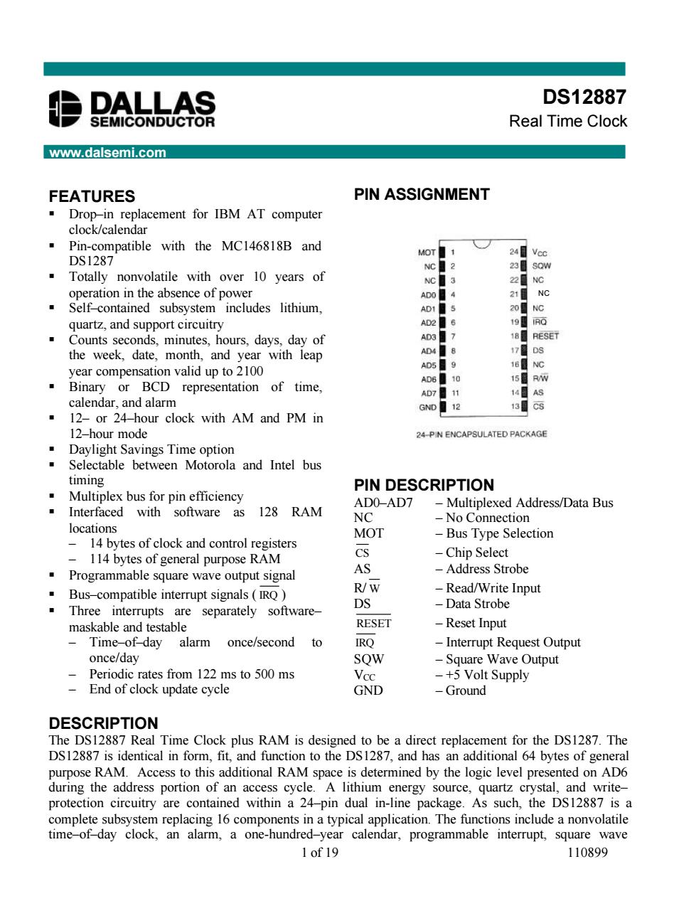
DAaba DS12887 Real Time Clock www.dalsemi.com FEATURES PIN ASSIGNMENT Drop-in replacement for IBM AT computer clock/calendar Pin-compatible with the MC146818B and DS1287 MOT Totally nonvolatile with over 10 years of omeymcethu. 24 NC quartz.and support circuitry ■Counts seco Is minutes hours days day of AD3 RESE the week.date.month.and ear with leap AD4 R representation of time, 14 AS GND12 13■c 1 ur clock with AM and PM in 24-PIN ENCAPSULATED PACKAGE Selectable between Motorola and Intel bus PIN DESCRIPTION Multiplex bus for pin efficiency AD7 .Interfaced with software as 128 RAM Multiplexed Address/Data Bus locations lection 14 bytes of clock and control registers Cs 114 bytes of general purpose RAM -Chip Select .Programmable square wave output signal AS -Address Strobe compatible interrupt signals(RQ) R/W -Read/Write Input DS Data Strobe interrupts are separately software- maskable and testable RESET -Reset Input Time-of-day alarm once/second to IRO -Interrupt Request Output once/day SOW -Square Wave Output Periodic rates from 122 ms to 500 ms -+5 Volt Supply End of clock update cycle GND -Ground DESCRIPTION DS12887 Real Time Clock plus RAM is designed to be a direct replacement for the DS1287.Th D17is identical in fom,it and tunction to the DS1287,and has anaddtonal64bytes of general purpose RAM.Access to this additional RAM space is determined by the logic level presented on AD6 during the address portion of an access cycle.A lithium energy source,quartz crystal,and write- protection circuitry are contained within a 24-pin dual in-line package.As such,the DS12887 is a complete subsystem replacing 16 components in a typical application.The functions include a nonvolatile time-of day clock,an alarm,a one-hundred-year calendar,programmable interrupt,square wave 1of19 110899 1 of 19 110899 FEATURES ß Drop–in replacement for IBM AT computer clock/calendar ß Pin-compatible with the MC146818B and DS1287 ß Totally nonvolatile with over 10 years of operation in the absence of power ß Self–contained subsystem includes lithium, quartz, and support circuitry ß Counts seconds, minutes, hours, days, day of the week, date, month, and year with leap year compensation valid up to 2100 ß Binary or BCD representation of time, calendar, and alarm ß 12– or 24–hour clock with AM and PM in 12–hour mode ß Daylight Savings Time option ß Selectable between Motorola and Intel bus timing ß Multiplex bus for pin efficiency ß Interfaced with software as 128 RAM locations – 14 bytes of clock and control registers – 114 bytes of general purpose RAM ß Programmable square wave output signal ß Bus–compatible interrupt signals ( IRQ ) ß Three interrupts are separately software– maskable and testable – Time–of–day alarm once/second to once/day – Periodic rates from 122 ms to 500 ms – End of clock update cycle PIN ASSIGNMENT PIN DESCRIPTION AD0–AD7 – Multiplexed Address/Data Bus NC – No Connection MOT – Bus Type Selection CS – Chip Select AS – Address Strobe R/ W – Read/Write Input DS – Data Strobe RESET – Reset Input IRQ – Interrupt Request Output SQW – Square Wave Output VCC – +5 Volt Supply GND – Ground DESCRIPTION The DS12887 Real Time Clock plus RAM is designed to be a direct replacement for the DS1287. The DS12887 is identical in form, fit, and function to the DS1287, and has an additional 64 bytes of general purpose RAM. Access to this additional RAM space is determined by the logic level presented on AD6 during the address portion of an access cycle. A lithium energy source, quartz crystal, and write– protection circuitry are contained within a 24–pin dual in-line package. As such, the DS12887 is a complete subsystem replacing 16 components in a typical application. The functions include a nonvolatile time–of–day clock, an alarm, a one-hundred–year calendar, programmable interrupt, square wave NC DS12887 Real Time Clock www.dalsemi.com