正在加载图片...
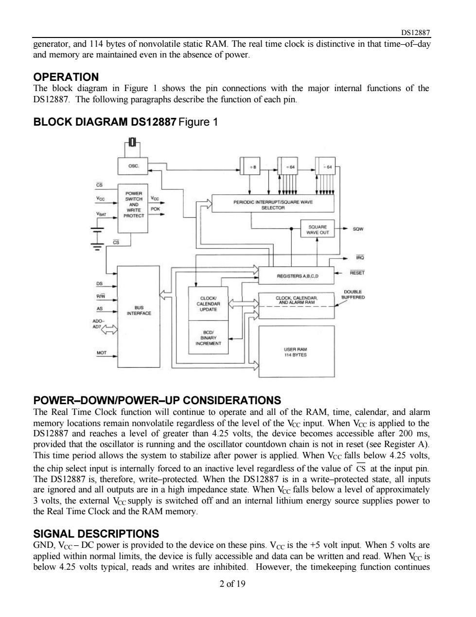
DS12887 .and 11 by e of nonvolatile static RAM.The real time clock is distinctive in that time-of day and memory are maintained even in the absence of power OPERATION The block diagram in Figure 1 shows the pin connections with the major internal functions of the DS12887.The following paragraphs describe the function of each pin. BLOCK DIAGRAM DS12887 Figure 1 AS POWER-DOWN/POWER-UP CONSIDERATIONS The Real Time Clock function will continue to operate and all of the RAM,time,calendar,and alarm memory locations remain nonvolatile regardless of the level of the Voc input.When Vcc is applied to the DS12887 and reaches a level of greater than 4.25 volts,the device becomes accessible after 200 ms provided that the oscillator is running and the oscillator countdown chain is not in reset(see Register A). This time period allows the system to stabilize after power is applied.When Vcc falls below 4.25 volts, slect in is inmlly forced toe the input pin state,all are ignored and al nce state kR8ne8Re资新mof nd anmeryour SIGNAL DESCRIPTIONS GND,Vcc-DC power is provided to the device on these pins.Vcc is the +5 volt input.When 5 volts are 2of19DS12887 2 of 19 generator, and 114 bytes of nonvolatile static RAM. The real time clock is distinctive in that time–of–day and memory are maintained even in the absence of power. OPERATION The block diagram in Figure 1 shows the pin connections with the major internal functions of the DS12887. The following paragraphs describe the function of each pin. BLOCK DIAGRAM DS12887 Figure 1 POWER–DOWN/POWER–UP CONSIDERATIONS The Real Time Clock function will continue to operate and all of the RAM, time, calendar, and alarm memory locations remain nonvolatile regardless of the level of the VCC input. When VCC is applied to the DS12887 and reaches a level of greater than 4.25 volts, the device becomes accessible after 200 ms, provided that the oscillator is running and the oscillator countdown chain is not in reset (see Register A). This time period allows the system to stabilize after power is applied. When VCC falls below 4.25 volts, the chip select input is internally forced to an inactive level regardless of the value of CS at the input pin. The DS12887 is, therefore, write–protected. When the DS12887 is in a write–protected state, all inputs are ignored and all outputs are in a high impedance state. When VCC falls below a level of approximately 3 volts, the external VCC supply is switched off and an internal lithium energy source supplies power to the Real Time Clock and the RAM memory. SIGNAL DESCRIPTIONS GND, VCC – DC power is provided to the device on these pins. VCC is the +5 volt input. When 5 volts are applied within normal limits, the device is fully accessible and data can be written and read. When VCC is below 4.25 volts typical, reads and writes are inhibited. However, the timekeeping function continues