正在加载图片...
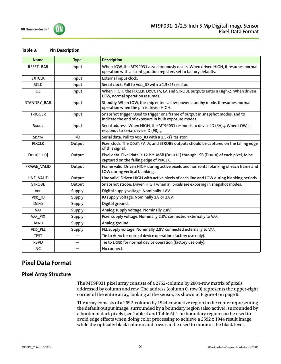
Mw9Po311/251hcn5MDeaelDgaeSnmat Table3: Pin Description Name Description RESET_BAR Input pperation with all configuration registers set to factory defaults. HIGH,it resumes norm EXTCIK Input xternal input clock. SCIK Input erial clock pull to Voo lowith a 1 5ko resistor OE Input STANDBY_BAR Input TRIGGER Input in snapshot modesandto SADDR Input erial add to device ID(BA)When LOW,it SDATA 1/o erial data.Pull to VoD O with a 1.5k resistor. PIXCLK Output el clock.The DoUT,FV,LV,and STROBE outputs should be captured on the falling edge of this signal. DoUT[11:0] Output Pixel data.Pixel data is 12-bit.MSB(DoUT11)through LSB(DoUTO)of each pixel,to be captured on the falling edge of PIXCL FRAME_VALID Output oWiUalgemealtlGndlrim8actepiesandhoromtalblankingofeachfameand Output lid Drive ve pi els of each line and LOW during bla ng periods. Output n HIGH wher ll pixels are exposing in snapshot modes Supply Digital supply voltage.Nominally 18V Supply Osupply voltage.Nominally 1.8 or 2.8V. DGND Supply Digital ground. VAA Supply Analog supply voltage.Nominally 2.8V. VAA PIX Supply Pixel supply voltage.Nominally 2.8V,connected externally to VAA. AGND Supply Analog ground. VDD_PLL Supply PLLsupply voltage.Nominally 2.8V,connected externally to VAA. TEST Tie to AGND for normal device operation(factory use only). RSVD ie to dGND for normal device operation (factory use onlyi No connect. Pixel Data Format Pixel Array Structure eoeneakgeaagEgogegrerne addre Ttearpycensitsofa25e92.com9boateg2aaeeetedeb the de of daput e su0endedbYabb加5ndagego (a d to avoid edge effects when doing color processing to achieve a 2592x 1944 result image while the optically black column and rows can be used to monitor the black level. MTP00S EN MT9P031_DS Rev. J 5/15 EN 8 ©Semiconductor Components Industries, LLC,2015. MT9P031: 1/2.5-Inch 5 Mp Digital Image Sensor Pixel Data Format Pixel Data Format Pixel Array Structure The MT9P031 pixel array consists of a 2752-column by 2004-row matrix of pixels addressed by column and row. The address (column 0, row 0) represents the upper-right corner of the entire array, looking at the sensor, as shown in Figure 4 on page 9. The array consists of a 2592-column by 1944-row active region in the center representing the default output image, surrounded by a boundary region (also active), surrounded by a border of dark pixels (see Table 4 and Table 5). The boundary region can be used to avoid edge effects when doing color processing to achieve a 2592 x 1944 result image, while the optically black column and rows can be used to monitor the black level. Table 3: Pin Description Name Type Description RESET_BAR Input When LOW, the MT9P031 asynchronously resets. When driven HIGH, it resumes normal operation with all configuration registers set to factory defaults. EXTCLK Input External input clock. SCLK Input Serial clock. Pull to VDD_IO with a 1.5k resistor. OE Input When HIGH, the PIXCLK, DOUT, FV, LV, and STROBE outputs enter a High-Z. When driven LOW, normal operation resumes. STANDBY_BAR Input Standby. When LOW, the chip enters a low-power standby mode. It resumes normal operation when the pin is driven HIGH. TRIGGER Input Snapshot trigger. Used to trigger one frame of output in snapshot modes, and to indicate the end of exposure in bulb exposure modes. SADDR Input Serial address. When HIGH, the MT9P031 responds to device ID (BA)H. When LOW, it responds to serial device ID (90)H. SDATA I/O Serial data. Pull to VDD_IO with a 1.5k resistor. PIXCLK Output Pixel clock. The DOUT, FV, LV, and STROBE outputs should be captured on the falling edge of this signal. DOUT[11:0] Output Pixel data. Pixel data is 12-bit. MSB (DOUT11) through LSB (DOUT0) of each pixel, to be captured on the falling edge of PIXCLK. FRAME_VALID Output Frame valid. Driven HIGH during active pixels and horizontal blanking of each frame and LOW during vertical blanking. LINE_VALID Output Line valid. Driven HIGH with active pixels of each line and LOW during blanking periods. STROBE Output Snapshot strobe. Driven HIGH when all pixels are exposing in snapshot modes. VDD Supply Digital supply voltage. Nominally 1.8V. VDD_IO Supply IO supply voltage. Nominally 1.8 or 2.8V. DGND Supply Digital ground. VAA Supply Analog supply voltage. Nominally 2.8V. VAA_PIX Supply Pixel supply voltage. Nominally 2.8V, connected externally to VAA. AGND Supply Analog ground. VDD_PLL Supply PLL supply voltage. Nominally 2.8V, connected externally to VAA. TEST — Tie to AGND for normal device operation (factory use only). RSVD — Tie to DGND for normal device operation (factory use only). NC — No connect