正在加载图片...
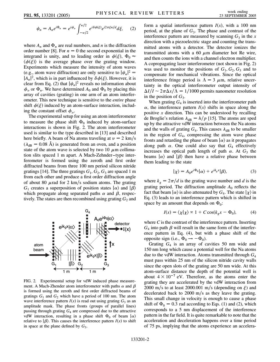
week ending PRL95,133201(2005) PHYSICAL REVIEW LETTERS 23 SEPTEMBER 2005 中n=Anei地。a=e冲。 w/2 ei8o()ermen/ddE, form a spatial interference pattern I(x).with a 100 nm (2) -w/2 period,at the plane of G3.The phase and contrast of the interference pattern are measured by scanning Ga in the x direction with a piezoelectric stage and counting the trans- where A,and d are real numbers,and n is the diffraction mitted atoms with a detector.The detector ionizes the order number [8].For n =0 the second exponential in the transmitted atoms with a 60 um diameter hot Re wire, integrand is unity,.and to leading order in中(),Φo≈ and then counts the ions with a channel electron multiplier. (()is the average phase over the grating window. Experiments which measure the intensity of atom waves A copropagating laser interferometer(not shown in Fig.2) was used to monitor the positions of G1,G2,G3 and to (e.g.,atom wave diffraction)are only sensitive to2= compensate for mechanical vibrations.Since the optical IA2,which is in part influenced by ()However,it is interference fringe period is A=3 um,relative uncer- clear from Eq.(2)that2 reveals no information about tainty in the optical interferometer output intensity of 中oorΦn.We have determined Ao andΦby placing this AlI~2Ax/A 1/1000 permits nanometer resolution array of cavities (grating)in one arm of an atom interfer- in the position of G3. ometer.This new technique is sensitive to the entire phase When grating G4 is inserted into the interferometer path shift ()induced by an atom-surface interaction,includ- a,the interference pattern I(x)shifts in space along the ing the constant offset中。 positive x direction.This can be understood by recalling The experimental setup for using an atom interferometer de Broglie's relation AdB =h/p [15].The atoms are sped to measure the phase shift Po induced by atom-surface up by the attractive vdW interaction between the Na atoms interactions is shown in Fig.2.The atom interferometer and the walls of grating G4.This causes AdB to be smaller used is similar to the type described in [13]and described in the region of G4,compressing the atom wave phase here briefly.A beam of Na atoms traveling at v =2 km/s fronts and retarding the phase of beam la)as it propagates (AdB =0.08 A)is generated from an oven,and a position along path a.One could also say that G4 effectively state of the atom wave is selected by two 10 um collima- increases the optical path length of path a.At G3 the tion slits spaced 1 m apart.A Mach-Zehnder-type inter- beams la)and IB)then have a relative phase between ferometer is formed using the zeroth and first order them leading to the state diffracted beams from three 100 nm period silicon nitride gratings [14].The three gratings G1,G2,G3 are spaced 1 m lx〉=Aneiola〉+ekB), (3) from each other and produce a first order diffraction angle of about 80 urad for 2 km/s sodium atoms.The grating where k=2/d is the grating wave number and d is the GI creates a superposition of position states la)and IB) grating period.The diffraction amplitude Ao reflects the which propagate along separated paths a and B,respec- fact that beam la)is also attenuated by G4.The state lx)in tively.The states are then recombined using grating G2 and Eg.(3)leads to an interference pattern which is shifted in space by an amount that depends on Po: G I(x)=(XlX〉x1+Ccos(kgx-Φo), (4) Aoeio) detector where C is the contrast of the interference pattern.Inserting ●I(X) G4 into path B will result in the same form of the interfer- ence pattern in Eq.(4),but with a phase shift of the opposite sign(i.e,Φo一-Φo). atom Grating G4 is an array of cavities 50 nm wide and beam ◆ 150 nm long which cause a potential well for the Na atoms eikgxβ> due to the vdW interaction.Atoms transmitted through G4 ◆ must pass within 25 nm of the silicon nitride cavity walls Iβ> G since the open slots of the grating are 50 nm wide.At this 1m 1m atom-surface distance the depth of the potential well is about 4X 10⁻⁷ eV.Therefore,as the atoms enter the FIG.2.Experimental setup for vdw induced phase measure- grating they are accelerated by the vdW interaction from ment.A Mach-Zhender atom interferometer with paths a and B 2000 m/s to at least 2000.001 m/s (depending on and is formed using the zeroth and first order diffracted beams of gratings Gi and G2 which have a period of 100 nm.The atom decelerated back to 2000 m/s as they leave the grating. wave interference pattern I(x)is read out using grating G3 as an This small change in velocity is enough to cause a phase amplitude mask.The phase fronts (groups of parallel lines) shift of o=0.3 rad according to Eqs.(1)and (2),which passing through grating G4 are compressed due to the attractive corresponds to a 5 nm displacement of the interference vdW interaction,resulting in a phase shift Po of beam la) pattern in the far field.It is quite remarkable to note that the relative to B).This causes the interference pattern I(x)to shift acceleration and deceleration happens over a time period in space at the plane defined by G3. of 75 ps,implying that the atoms experience an accelera- 133201-2n Anein eio Z w=2 w=2 ei ei2n=dd; (2) where An and n are real numbers, and n is the diffraction order number [8]. For n 0 the second exponential in the integrand is unity, and to leading order in , 0 hi is the average phase over the grating window. Experiments which measure the intensity of atom waves (e.g., atom wave diffraction) are only sensitive to j nj 2 jAnj 2, which is in part influenced by . However, it is clear from Eq. (2) that j nj 2 reveals no information about o or n. We have determined A0 and 0 by placing this array of cavities (grating) in one arm of an atom interferometer. This new technique is sensitive to the entire phase shift induced by an atom-surface interaction, including the constant offset o. The experimental setup for using an atom interferometer to measure the phase shift 0 induced by atom-surface interactions is shown in Fig. 2. The atom interferometer used is similar to the type described in [13] and described here briefly. A beam of Na atoms traveling at v 2 km=s (dB 0:08 A ) is generated from an oven, and a position state of the atom wave is selected by two 10 m collimation slits spaced 1 m apart. A Mach-Zehnder –type interferometer is formed using the zeroth and first order diffracted beams from three 100 nm period silicon nitride gratings [14]. The three gratings G1; G2; G3 are spaced 1 m from each other and produce a first order diffraction angle of about 80 rad for 2 km=s sodium atoms. The grating G1 creates a superposition of position states ji and ji which propagate along separated paths and , respectively. The states are then recombined using grating G2 and form a spatial interference pattern Ix, with a 100 nm period, at the plane of G3. The phase and contrast of the interference pattern are measured by scanning G3 in the x direction with a piezoelectric stage and counting the transmitted atoms with a detector. The detector ionizes the transmitted atoms with a 60 m diameter hot Re wire, and then counts the ions with a channel electron multiplier. A copropagating laser interferometer (not shown in Fig. 2) was used to monitor the positions of G1; G2; G3 and to compensate for mechanical vibrations. Since the optical interference fringe period is 3 m, relative uncertainty in the optical interferometer output intensity of I=I 2x= 1=1000 permits nanometer resolution in the position of G3. When grating G4 is inserted into the interferometer path , the interference pattern Ix shifts in space along the positive x direction. This can be understood by recalling de Broglie’s relation dB h=p [15]. The atoms are sped up by the attractive vdW interaction between the Na atoms and the walls of grating G4. This causes dB to be smaller in the region of G4, compressing the atom wave phase fronts and retarding the phase of beam ji as it propagates along path . One could also say that G4 effectively increases the optical path length of path . At G3 the beams ji and ji then have a relative phase between them leading to the state j i A0ei0 ji eikgxji; (3) where kg 2=d is the grating wave number and d is the grating period. The diffraction amplitude A0 reflects the fact that beam ji is also attenuated by G4. The state j i in Eq. (3) leads to an interference pattern which is shifted in space by an amount that depends on 0: Ixh j i / 1 Ccoskgx 0; (4) where C is the contrast of the interference pattern. Inserting G4 into path will result in the same form of the interference pattern in Eq. (4), but with a phase shift of the opposite sign (i.e., 0 ! 0). Grating G4 is an array of cavities 50 nm wide and 150 nm long which cause a potential well for the Na atoms due to the vdW interaction. Atoms transmitted through G4 must pass within 25 nm of the silicon nitride cavity walls since the open slots of the grating are 50 nm wide. At this atom-surface distance the depth of the potential well is about 4 107 eV. Therefore, as the atoms enter the grating they are accelerated by the vdW interaction from 2000 m=s to at least 2000:001 m=s (depending on ) and decelerated back to 2000 m=s as they leave the grating. This small change in velocity is enough to cause a phase shift of 0 0:3 rad according to Eqs. (1) and (2), which corresponds to a 5 nm displacement of the interference pattern in the far field. It is quite remarkable to note that the acceleration and deceleration happens over a time period of 75 ps, implying that the atoms experience an acceleraatom beam G1 G2 G3 G4 x I(x) detector eikgx A0eiΦ0 eikgx|α> |β> |α> |β> 1 m 1 m FIG. 2. Experimental setup for vdW induced phase measurement. A Mach-Zhender atom interferometer with paths and is formed using the zeroth and first order diffracted beams of gratings G1 and G2 which have a period of 100 nm. The atom wave interference pattern Ix is read out using grating G3 as an amplitude mask. The phase fronts (groups of parallel lines) passing through grating G4 are compressed due to the attractive vdW interaction, resulting in a phase shift 0 of beam ji relative to ji. This causes the interference pattern Ix to shift in space at the plane defined by G3. PRL 95, 133201 (2005) PHYSICAL REVIEW LETTERS week ending 23 SEPTEMBER 2005 133201-2�������������������������������������������