正在加载图片...
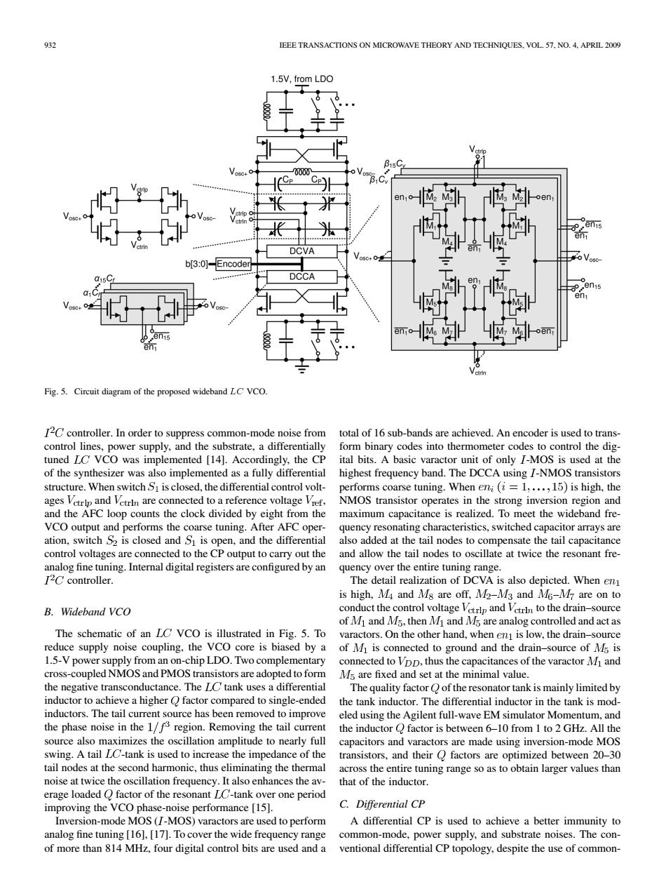
932 IEEE TRANSACTIONS ON MICROWAVE THEORY AND TECHNIQUES.VOL.57.NO.4.APRIL 2009 1.5V,from LDO B15C -0000 an鸠 区en b[3:0]-Encode 015 h 感4丽 Fig.5.Circuit diagram of the proposed wideband LC VCO. 12C controller.In order to suppress common-mode noise from total of 16 sub-bands are achieved.An encoder is used to trans- control lines,power supply,and the substrate,a differentially form binary codes into thermometer codes to control the dig- tuned LC VCO was implemented [14].Accordingly,the CP ital bits.A basic varactor unit of only I-MOS is used at the of the synthesizer was also implemented as a fully differential highest frequency band.The DCCA using I-NMOS transistors structure.When switch S is closed,the differential control volt- performs coarse tuning.When eni(=1,...,15)is high,the ages Vtrlp and Vetrin are connected to a reference voltage Vief, NMOS transistor operates in the strong inversion region and and the AFC loop counts the clock divided by eight from the maximum capacitance is realized.To meet the wideband fre- VCO output and performs the coarse tuning.After AFC oper- quency resonating characteristics,switched capacitor arrays are ation,switch S2 is closed and S is open,and the differential also added at the tail nodes to compensate the tail capacitance control voltages are connected to the CP output to carry out the and allow the tail nodes to oscillate at twice the resonant fre- analog fine tuning.Internal digital registers are configured by an quency over the entire tuning range. T2C controller. The detail realization of DCVA is also depicted.When en is high,Ma and Ms are off,M2-M3 and M6-M7 are on to B.Wideband VCO conduct the control voltage Vetrlp and Vetrin to the drain-source of M and M5,then Mi and M5 are analog controlled and act as The schematic of an LC VCO is illustrated in Fig.5.To varactors.On the other hand,when en is low,the drain-source reduce supply noise coupling,the VCO core is biased by a of M is connected to ground and the drain-source of M is 1.5-V power supply from an on-chip LDO.Two complementary connected to Vpp,thus the capacitances of the varactor Mi and cross-coupled NMOS and PMOS transistors are adopted to form Ms are fixed and set at the minimal value. the negative transconductance.The LC tank uses a differential The quality factor Q of the resonator tank is mainly limited by inductor to achieve a higher O factor compared to single-ended the tank inductor.The differential inductor in the tank is mod- inductors.The tail current source has been removed to improve eled using the Agilent full-wave EM simulator Momentum,and the phase noise in the 1/f3 region.Removing the tail current the inductor Q factor is between 6-10 from 1 to 2 GHz.All the source also maximizes the oscillation amplitude to nearly full capacitors and varactors are made using inversion-mode MOS swing.A tail LC-tank is used to increase the impedance of the transistors,and their factors are optimized between 20-30 tail nodes at the second harmonic,thus eliminating the thermal across the entire tuning range so as to obtain larger values than noise at twice the oscillation frequency.It also enhances the av-that of the inductor. erage loaded Q factor of the resonant LC-tank over one period improving the VCO phase-noise performance [15]. C.Differential CP Inversion-mode MOS(I-MOS)varactors are used to perform A differential CP is used to achieve a better immunity to analog fine tuning [16],[17].To cover the wide frequency range common-mode,power supply,and substrate noises.The con- of more than 814 MHz,four digital control bits are used and a ventional differential CP topology,despite the use of common-932 IEEE TRANSACTIONS ON MICROWAVE THEORY AND TECHNIQUES, VOL. 57, NO. 4, APRIL 2009 Fig. 5. Circuit diagram of the proposed wideband VCO. controller. In order to suppress common-mode noise from control lines, power supply, and the substrate, a differentially tuned VCO was implemented [14]. Accordingly, the CP of the synthesizer was also implemented as a fully differential structure. When switch is closed, the differential control voltages and are connected to a reference voltage , and the AFC loop counts the clock divided by eight from the VCO output and performs the coarse tuning. After AFC operation, switch is closed and is open, and the differential control voltages are connected to the CP output to carry out the analog fine tuning. Internal digital registers are configured by an controller. B. Wideband VCO The schematic of an VCO is illustrated in Fig. 5. To reduce supply noise coupling, the VCO core is biased by a 1.5-V power supply from an on-chip LDO. Two complementary cross-coupled NMOS and PMOS transistors are adopted to form the negative transconductance. The tank uses a differential inductor to achieve a higher factor compared to single-ended inductors. The tail current source has been removed to improve the phase noise in the region. Removing the tail current source also maximizes the oscillation amplitude to nearly full swing. A tail -tank is used to increase the impedance of the tail nodes at the second harmonic, thus eliminating the thermal noise at twice the oscillation frequency. It also enhances the average loaded factor of the resonant -tank over one period improving the VCO phase-noise performance [15]. Inversion-mode MOS ( -MOS) varactors are used to perform analog fine tuning [16], [17]. To cover the wide frequency range of more than 814 MHz, four digital control bits are used and a total of 16 sub-bands are achieved. An encoder is used to transform binary codes into thermometer codes to control the digital bits. A basic varactor unit of only -MOS is used at the highest frequency band. The DCCA using -NMOS transistors performs coarse tuning. When is high, the NMOS transistor operates in the strong inversion region and maximum capacitance is realized. To meet the wideband frequency resonating characteristics, switched capacitor arrays are also added at the tail nodes to compensate the tail capacitance and allow the tail nodes to oscillate at twice the resonant frequency over the entire tuning range. The detail realization of DCVA is also depicted. When is high, and are off, – and – are on to conduct the control voltage and to the drain–source of and , then and are analog controlled and act as varactors. On the other hand, when is low, the drain–source of is connected to ground and the drain–source of is connected to , thus the capacitances of the varactor and are fixed and set at the minimal value. The quality factor of the resonator tank is mainly limited by the tank inductor. The differential inductor in the tank is modeled using the Agilent full-wave EM simulator Momentum, and the inductor factor is between 6–10 from 1 to 2 GHz. All the capacitors and varactors are made using inversion-mode MOS transistors, and their factors are optimized between 20–30 across the entire tuning range so as to obtain larger values than that of the inductor. C. Differential CP A differential CP is used to achieve a better immunity to common-mode, power supply, and substrate noises. The conventional differential CP topology, despite the use of common-�