正在加载图片...
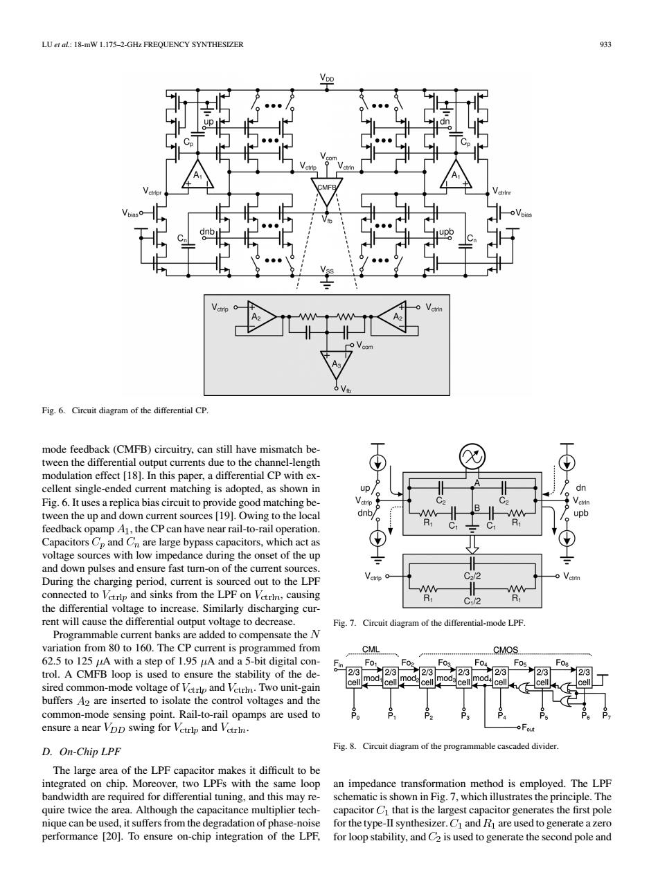
LU et al:18-mW 1.175-2-GHz FREQUENCY SYNTHESIZER 933 VDD T9 h Fig.6.Circuit diagram of the differential CP. mode feedback(CMFB)circuitry,can still have mismatch be- tween the differential output currents due to the channel-length modulation effect [18].In this paper,a differential CP with ex- cellent single-ended current matching is adopted,as shown in up dn Fig.6.It uses a replica bias circuit to provide good matching be- tween the up and down current sources [19].Owing to the local dnb/ upb feedback opamp A1,the CP can have near rail-to-rail operation. Capacitors Cp and Cn are large bypass capacitors,which act as voltage sources with low impedance during the onset of the up and down pulses and ensure fast turn-on of the current sources. C2/2 During the charging period,current is sourced out to the LPF W connected to Vetrlp and sinks from the LPF on Vetrin,causing -M C1/2 R1 the differential voltage to increase.Similarly discharging cur- rent will cause the differential output voltage to decrease. Fig.7.Circuit diagram of the differential-mode LPF Programmable current banks are added to compensate the N variation from 80 to 160.The CP current is programmed from CML CMOS 62.5 to 125 uA with a step of 1.95 uA and a 5-bit digital con- F02 Fos trol.A CMFB loop is used to ensure the stability of the de- 2/3 231 23 23 23 23 213 ell sired common-mode voltage of Vetrlp and Vetrl.Two unit-gain cell mod:cell modacell buffers A2 are inserted to isolate the control voltages and the common-mode sensing point.Rail-to-rail opamps are used to Pa ensure a near VDD swing for Vetrlp and Vetrin. D.On-Chip LPF Fig.8.Circuit diagram of the programmable cascaded divider. The large area of the LPF capacitor makes it difficult to be integrated on chip.Moreover,two LPFs with the same loop an impedance transformation method is employed.The LPF bandwidth are required for differential tuning,and this may re- schematic is shown in Fig.7,which illustrates the principle.The quire twice the area.Although the capacitance multiplier tech-capacitor Cl that is the largest capacitor generates the first pole nique can be used,it suffers from the degradation of phase-noise for the type-II synthesizer.Ci and R are used to generate a zero performance [20].To ensure on-chip integration of the LPF, for loop stability,and C2 is used to generate the second pole andLU et al.: 18-mW 1.175–2-GHz FREQUENCY SYNTHESIZER 933 Fig. 6. Circuit diagram of the differential CP. mode feedback (CMFB) circuitry, can still have mismatch between the differential output currents due to the channel-length modulation effect [18]. In this paper, a differential CP with excellent single-ended current matching is adopted, as shown in Fig. 6. It uses a replica bias circuit to provide good matching between the up and down current sources [19]. Owing to the local feedback opamp , the CP can have near rail-to-rail operation. Capacitors and are large bypass capacitors, which act as voltage sources with low impedance during the onset of the up and down pulses and ensure fast turn-on of the current sources. During the charging period, current is sourced out to the LPF connected to and sinks from the LPF on , causing the differential voltage to increase. Similarly discharging current will cause the differential output voltage to decrease. Programmable current banks are added to compensate the variation from 80 to 160. The CP current is programmed from 62.5 to 125 A with a step of 1.95 A and a 5-bit digital control. A CMFB loop is used to ensure the stability of the desired common-mode voltage of and . Two unit-gain buffers are inserted to isolate the control voltages and the common-mode sensing point. Rail-to-rail opamps are used to ensure a near swing for and . D. On-Chip LPF The large area of the LPF capacitor makes it difficult to be integrated on chip. Moreover, two LPFs with the same loop bandwidth are required for differential tuning, and this may require twice the area. Although the capacitance multiplier technique can be used, it suffers from the degradation of phase-noise performance [20]. To ensure on-chip integration of the LPF, Fig. 7. Circuit diagram of the differential-mode LPF. Fig. 8. Circuit diagram of the programmable cascaded divider. an impedance transformation method is employed. The LPF schematic is shown in Fig. 7, which illustrates the principle. The capacitor that is the largest capacitor generates the first pole for the type-II synthesizer. and are used to generate a zero for loop stability, and is used to generate the second pole and