正在加载图片...
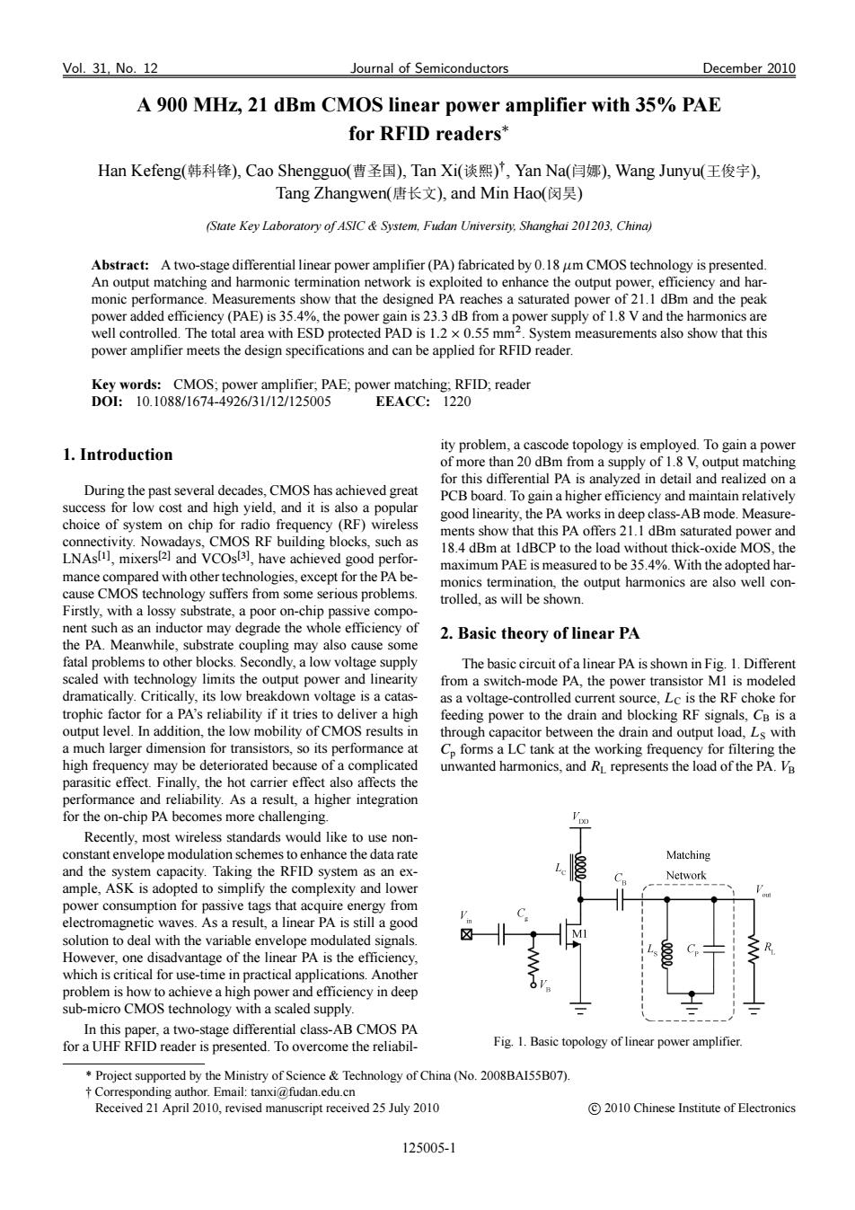
Vol.31,No.12 Journal of Semiconductors December 2010 A 900 MHz,21 dBm CMOS linear power amplifier with 35%PAE for RFID readers* Han Kefeng(韩科锋),Cao Shengguo(曹圣国),Tan Xi(谈熙)',Yan Na(闫娜),Wang Junyu(王俊宇), Tang Zhangwen(唐长文),and Min Hao(闵昊) (State Key Laboratory of ASIC System,Fudan University.Shanghai 201203,China) Abstract:A two-stage differential linear power amplifier(PA)fabricated by 0.18 um CMOS technology is presented. An output matching and harmonic termination network is exploited to enhance the output power,efficiency and har- monic performance.Measurements show that the designed PA reaches a saturated power of 21.1 dBm and the peak power added efficiency(PAE)is 35.4%,the power gain is 23.3 dB from a power supply of 1.8 Vand the harmonics are well controlled.The total area with ESD protected PAD is 1.2 x 0.55 mm2.System measurements also show that this power amplifier meets the design specifications and can be applied for RFID reader. Key words:CMOS;power amplifier;PAE;power matching;RFID;reader D0:10.1088/1674-4926/31/12/125005 EEACC:1220 ity problem,a cascode topology is employed.To gain a power 1.Introduction of more than 20 dBm from a supply of 1.8 V,output matching for this differential PA is analyzed in detail and realized on a During the past several decades,CMOS has achieved great PCB board.To gain a higher efficiency and maintain relatively success for low cost and high yield,and it is also a popular good linearity,the PA works in deep class-AB mode.Measure- choice of system on chip for radio frequency (RF)wireless ments show that this PA offers 21.1 dBm saturated power and connectivity.Nowadays,CMOS RF building blocks,such as 18.4 dBm at 1dBCP to the load without thick-oxide MOS,the LNAs[1],mixers[2]and VCOs[31,have achieved good perfor- maximum PAE is measured to be 35.4%.With the adopted har- mance compared with other technologies,except for the PA be- monics termination,the output harmonics are also well con- cause CMOS technology suffers from some serious problems. trolled,as will be shown. Firstly,with a lossy substrate,a poor on-chip passive compo- nent such as an inductor may degrade the whole efficiency of 2.Basic theory of linear PA the PA.Meanwhile,substrate coupling may also cause some fatal problems to other blocks.Secondly,a low voltage supply The basic circuit of a linear PA is shown in Fig.1.Different scaled with technology limits the output power and linearity from a switch-mode PA,the power transistor MI is modeled dramatically.Critically,its low breakdown voltage is a catas- as a voltage-controlled current source,Lc is the RF choke for trophic factor for a PA's reliability if it tries to deliver a high feeding power to the drain and blocking RF signals,CB is a output level.In addition,the low mobility of CMOS results in through capacitor between the drain and output load,Ls with a much larger dimension for transistors,so its performance at Cp forms a LC tank at the working frequency for filtering the high frequency may be deteriorated because of a complicated unwanted harmonics,and RL represents the load of the PA.VB parasitic effect.Finally,the hot carrier effect also affects the performance and reliability.As a result,a higher integration for the on-chip PA becomes more challenging. Recently,most wireless standards would like to use non- constant envelope modulation schemes to enhance the data rate Matching and the system capacity.Taking the RFID system as an ex- Network ample,ASK is adopted to simplify the complexity and lower power consumption for passive tags that acquire energy from electromagnetic waves.As a result,a linear PA is still a good solution to deal with the variable envelope modulated signals However,one disadvantage of the linear PA is the efficiency, which is critical for use-time in practical applications.Another problem is how to achieve a high power and efficiency in deep sub-micro CMOS technology with a scaled supply. In this paper,a two-stage differential class-AB CMOS PA for a UHF RFID reader is presented.To overcome the reliabil- Fig.1.Basic topology of linear power amplifier. *Project supported by the Ministry of Science&Technology of China(No.2008BAI55B07). Corresponding author.Email:tanxi@fudan.edu.cn Received 21 April 2010,revised manuscript received 25 July 2010 C2010 Chinese Institute of Electronics 125005-1Vol. 31, No. 12 Journal of Semiconductors December 2010 A 900 MHz, 21 dBm CMOS linear power amplifier with 35% PAE for RFID readers Han Kefeng(韩科锋), Cao Shengguo(曹圣国), Tan Xi(谈熙) , Yan Na(闫娜), Wang Junyu(王俊宇), Tang Zhangwen(唐长文), and Min Hao(闵昊) (State Key Laboratory of ASIC & System, Fudan University, Shanghai 201203, China) Abstract: A two-stage differential linear power amplifier (PA) fabricated by 0.18 m CMOS technology is presented. An output matching and harmonic termination network is exploited to enhance the output power, efficiency and harmonic performance. Measurements show that the designed PA reaches a saturated power of 21.1 dBm and the peak power added efficiency (PAE) is 35.4%, the power gain is 23.3 dB from a power supply of 1.8 V and the harmonics are well controlled. The total area with ESD protected PAD is 1:2 0:55 mm2 . System measurements also show that this power amplifier meets the design specifications and can be applied for RFID reader. Key words: CMOS; power amplifier; PAE; power matching; RFID; reader DOI: 10.1088/1674-4926/31/12/125005 EEACC: 1220 1. Introduction During the past several decades, CMOS has achieved great success for low cost and high yield, and it is also a popular choice of system on chip for radio frequency (RF) wireless connectivity. Nowadays, CMOS RF building blocks, such as LNAsŒ1, mixersŒ2 and VCOsŒ3, have achieved good performance compared with other technologies, except for the PA because CMOS technology suffers from some serious problems. Firstly, with a lossy substrate, a poor on-chip passive component such as an inductor may degrade the whole efficiency of the PA. Meanwhile, substrate coupling may also cause some fatal problems to other blocks. Secondly, a low voltage supply scaled with technology limits the output power and linearity dramatically. Critically, its low breakdown voltage is a catastrophic factor for a PA’s reliability if it tries to deliver a high output level. In addition, the low mobility of CMOS results in a much larger dimension for transistors, so its performance at high frequency may be deteriorated because of a complicated parasitic effect. Finally, the hot carrier effect also affects the performance and reliability. As a result, a higher integration for the on-chip PA becomes more challenging. Recently, most wireless standards would like to use nonconstant envelope modulation schemes to enhance the data rate and the system capacity. Taking the RFID system as an example, ASK is adopted to simplify the complexity and lower power consumption for passive tags that acquire energy from electromagnetic waves. As a result, a linear PA is still a good solution to deal with the variable envelope modulated signals. However, one disadvantage of the linear PA is the efficiency, which is critical for use-time in practical applications. Another problem is how to achieve a high power and efficiency in deep sub-micro CMOS technology with a scaled supply. In this paper, a two-stage differential class-AB CMOS PA for a UHF RFID reader is presented. To overcome the reliability problem, a cascode topology is employed. To gain a power of more than 20 dBm from a supply of 1.8 V, output matching for this differential PA is analyzed in detail and realized on a PCB board. To gain a higher efficiency and maintain relatively good linearity, the PA works in deep class-AB mode. Measurements show that this PA offers 21.1 dBm saturated power and 18.4 dBm at 1dBCP to the load without thick-oxide MOS, the maximum PAE is measured to be 35.4%. With the adopted harmonics termination, the output harmonics are also well controlled, as will be shown. 2. Basic theory of linear PA The basic circuit of a linear PA is shown in Fig. 1. Different from a switch-mode PA, the power transistor M1 is modeled as a voltage-controlled current source, LC is the RF choke for feeding power to the drain and blocking RF signals, CB is a through capacitor between the drain and output load, LS with Cp forms a LC tank at the working frequency for filtering the unwanted harmonics, and RL represents the load of the PA. VB Fig. 1. Basic topology of linear power amplifier. * Project supported by the Ministry of Science & Technology of China (No. 2008BAI55B07). Corresponding author. Email: tanxi@fudan.edu.cn Received 21 April 2010, revised manuscript received 25 July 2010 c 2010 Chinese Institute of Electronics 125005-1��