正在加载图片...
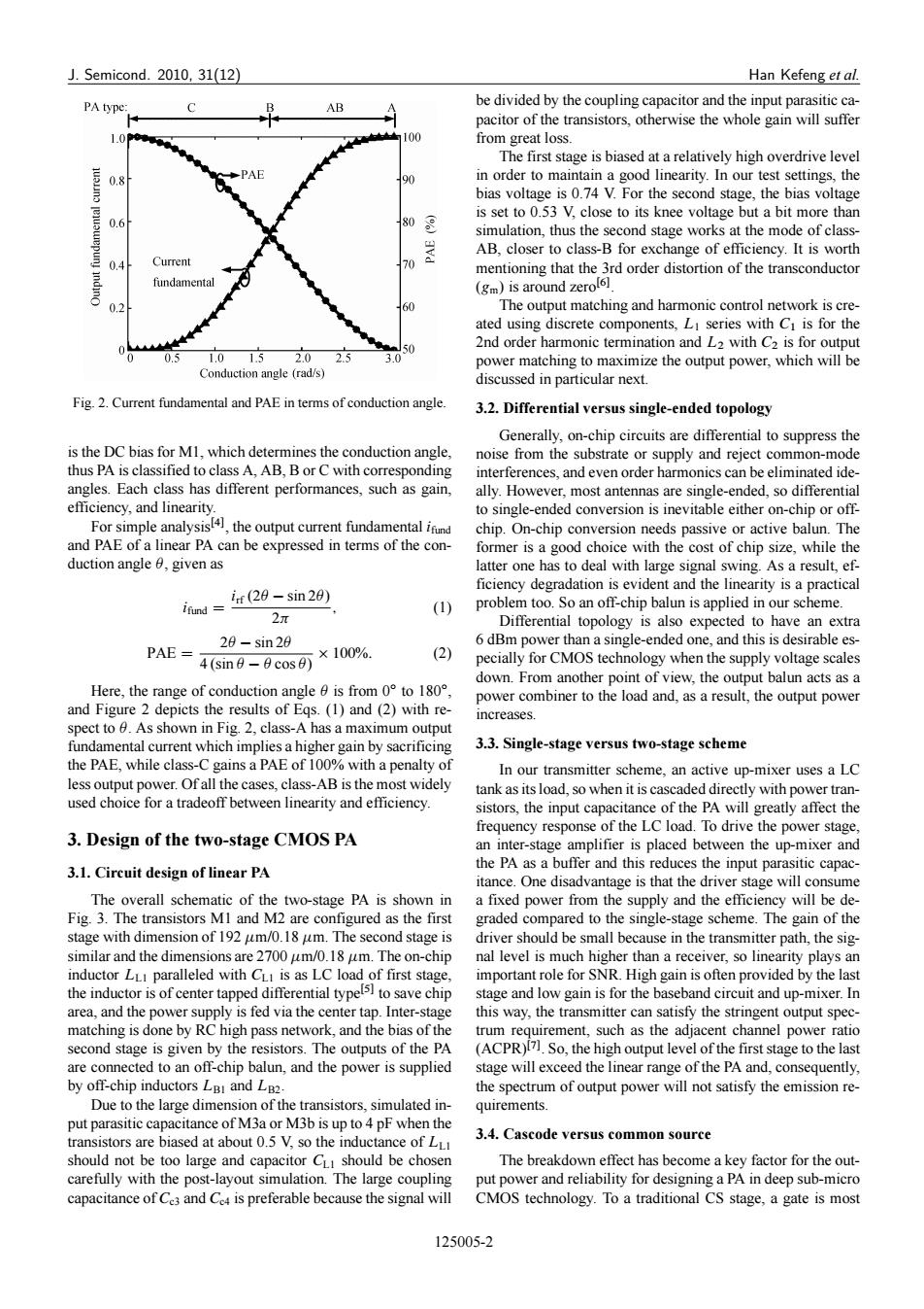
J.Semicond.2010,31(12) Han Kefeng et al. PA type: B AB be divided by the coupling capacitor and the input parasitic ca- pacitor of the transistors,otherwise the whole gain will suffer 1.0e 100 from great loss. The first stage is biased at a relatively high overdrive level 邑0.8 PAE 90 in order to maintain a good linearity.In our test settings,the bias voltage is 0.74 V.For the second stage,the bias voltage is set to 0.53 V.close to its knee voltage but a bit more than 0.6 80 simulation,thus the second stage works at the mode of class- AB,closer to class-B for exchange of efficiency.It is worth 0.4 Current 0 mentioning that the 3rd order distortion of the transconductor fundamental (gm)is around zerol6l. 0.2 60 The output matching and harmonic control network is cre- ated using discrete components,LI series with Cl is for the 50 2nd order harmonic termination and L2 with C2 is for output 0.5 1.0152.02.3 power matching to maximize the output power,which will be Conduction angle (rad/s) discussed in particular next. Fig.2.Current fundamental and PAE in terms of conduction angle. 3.2.Differential versus single-ended topology Generally,on-chip circuits are differential to suppress the is the DC bias for M1.which determines the conduction angle, noise from the substrate or supply and reject common-mode thus PA is classified to class A,AB,B or C with corresponding interferences,and even order harmonics can be eliminated ide- angles.Each class has different performances,such as gain, ally.However.most antennas are single-ended.so differential efficiency,and linearity. to single-ended conversion is inevitable either on-chip or off- For simple analysis,the output current fundamental id chip.On-chip conversion needs passive or active balun.The and PAE of a linear PA can be expressed in terms of the con- former is a good choice with the cost of chip size,while the duction angle 0,given as latter one has to deal with large signal swing.As a result,ef- innd =(20-sin20) ficiency degradation is evident and the linearity is a practical (1) problem too.So an off-chip balun is applied in our scheme. 2π Differential topology is also expected to have an extra 28-sin28 6 dBm power than a single-ended one,and this is desirable es- PAE= 4(sin9-6cos9×100%. (2) pecially for CMOS technology when the supply voltage scales down.From another point of view,the output balun acts as a Here,the range of conduction angle0 is from0°toI80°, power combiner to the load and,as a result,the output power and Figure 2 depicts the results of Egs.(1)and(2)with re- increases. spect to 0.As shown in Fig.2,class-A has a maximum output fundamental current which implies a higher gain by sacrificing 3.3.Single-stage versus two-stage scheme the PAE,while class-C gains a PAE of 100%with a penalty of In our transmitter scheme,an active up-mixer uses a LC less output power.Of all the cases,class-AB is the most widely tank as its load,so when it is cascaded directly with power tran- used choice for a tradeoff between linearity and efficiency. sistors,the input capacitance of the PA will greatly affect the frequency response of the LC load.To drive the power stage, 3.Design of the two-stage CMOS PA an inter-stage amplifier is placed between the up-mixer and the PA as a buffer and this reduces the input parasitic capac- 3.1.Circuit design of linear PA itance.One disadvantage is that the driver stage will consume The overall schematic of the two-stage PA is shown in a fixed power from the supply and the efficiency will be de- Fig.3.The transistors MI and M2 are configured as the first graded compared to the single-stage scheme.The gain of the stage with dimension of 192 um/0.18 um.The second stage is driver should be small because in the transmitter path,the sig- similar and the dimensions are 2700 um/0.18 um.The on-chip nal level is much higher than a receiver,so linearity plays an inductor LLI paralleled with CLI is as LC load of first stage, important role for SNR.High gain is often provided by the last the inductor is of center tapped differential typel5]to save chip stage and low gain is for the baseband circuit and up-mixer.In area,and the power supply is fed via the center tap.Inter-stage this way,the transmitter can satisfy the stringent output spec- matching is done by RC high pass network,and the bias of the trum requirement,such as the adjacent channel power ratio second stage is given by the resistors.The outputs of the PA (ACPR)7.So,the high output level of the first stage to the last are connected to an off-chip balun,and the power is supplied stage will exceed the linear range of the PA and,consequently, by off-chip inductors LBI and LB2. the spectrum of output power will not satisfy the emission re- Due to the large dimension of the transistors,simulated in- quirements. put parasitic capacitance of M3a or M3b is up to 4 pF when the transistors are biased at about 0.5 V,so the inductance of L 3.4.Cascode versus common source should not be too large and capacitor CLI should be chosen The breakdown effect has become a key factor for the out- carefully with the post-layout simulation.The large coupling put power and reliability for designing a PA in deep sub-micro capacitance of Ce3 and Co4 is preferable because the signal will CMOS technology.To a traditional CS stage,a gate is most 125005-2J. Semicond. 2010, 31(12) Han Kefeng et al. Fig. 2. Current fundamental and PAE in terms of conduction angle. is the DC bias for M1, which determines the conduction angle, thus PA is classified to class A, AB, B or C with corresponding angles. Each class has different performances, such as gain, efficiency, and linearity. For simple analysisŒ4, the output current fundamental ifund and PAE of a linear PA can be expressed in terms of the conduction angle , given as ifund D irf .2 sin 2 / 2 ; (1) PAE D 2 sin 2 4 .sin cos / 100%: (2) Here, the range of conduction angle is from 0ı to 180ı , and Figure 2 depicts the results of Eqs. (1) and (2) with respect to . As shown in Fig. 2, class-A has a maximum output fundamental current which implies a higher gain by sacrificing the PAE, while class-C gains a PAE of 100% with a penalty of less output power. Of all the cases, class-AB is the most widely used choice for a tradeoff between linearity and efficiency. 3. Design of the two-stage CMOS PA 3.1. Circuit design of linear PA The overall schematic of the two-stage PA is shown in Fig. 3. The transistors M1 and M2 are configured as the first stage with dimension of 192 m/0.18 m. The second stage is similar and the dimensions are 2700 m/0.18 m. The on-chip inductor LL1 paralleled with CL1 is as LC load of first stage, the inductor is of center tapped differential typeŒ5 to save chip area, and the power supply is fed via the center tap. Inter-stage matching is done by RC high pass network, and the bias of the second stage is given by the resistors. The outputs of the PA are connected to an off-chip balun, and the power is supplied by off-chip inductors LB1 and LB2. Due to the large dimension of the transistors, simulated input parasitic capacitance of M3a or M3b is up to 4 pF when the transistors are biased at about 0.5 V, so the inductance of LL1 should not be too large and capacitor CL1 should be chosen carefully with the post-layout simulation. The large coupling capacitance of Cc3 and Cc4 is preferable because the signal will be divided by the coupling capacitor and the input parasitic capacitor of the transistors, otherwise the whole gain will suffer from great loss. The first stage is biased at a relatively high overdrive level in order to maintain a good linearity. In our test settings, the bias voltage is 0.74 V. For the second stage, the bias voltage is set to 0.53 V, close to its knee voltage but a bit more than simulation, thus the second stage works at the mode of classAB, closer to class-B for exchange of efficiency. It is worth mentioning that the 3rd order distortion of the transconductor (gm/ is around zeroŒ6 . The output matching and harmonic control network is created using discrete components, L1 series with C1 is for the 2nd order harmonic termination and L2 with C2 is for output power matching to maximize the output power, which will be discussed in particular next. 3.2. Differential versus single-ended topology Generally, on-chip circuits are differential to suppress the noise from the substrate or supply and reject common-mode interferences, and even order harmonics can be eliminated ideally. However, most antennas are single-ended, so differential to single-ended conversion is inevitable either on-chip or offchip. On-chip conversion needs passive or active balun. The former is a good choice with the cost of chip size, while the latter one has to deal with large signal swing. As a result, efficiency degradation is evident and the linearity is a practical problem too. So an off-chip balun is applied in our scheme. Differential topology is also expected to have an extra 6 dBm power than a single-ended one, and this is desirable especially for CMOS technology when the supply voltage scales down. From another point of view, the output balun acts as a power combiner to the load and, as a result, the output power increases. 3.3. Single-stage versus two-stage scheme In our transmitter scheme, an active up-mixer uses a LC tank as its load, so when it is cascaded directly with power transistors, the input capacitance of the PA will greatly affect the frequency response of the LC load. To drive the power stage, an inter-stage amplifier is placed between the up-mixer and the PA as a buffer and this reduces the input parasitic capacitance. One disadvantage is that the driver stage will consume a fixed power from the supply and the efficiency will be degraded compared to the single-stage scheme. The gain of the driver should be small because in the transmitter path, the signal level is much higher than a receiver, so linearity plays an important role for SNR. High gain is often provided by the last stage and low gain is for the baseband circuit and up-mixer. In this way, the transmitter can satisfy the stringent output spectrum requirement, such as the adjacent channel power ratio (ACPR)Œ7. So, the high output level of the first stage to the last stage will exceed the linear range of the PA and, consequently, the spectrum of output power will not satisfy the emission requirements. 3.4. Cascode versus common source The breakdown effect has become a key factor for the output power and reliability for designing a PA in deep sub-micro CMOS technology. To a traditional CS stage, a gate is most 125005-2�