正在加载图片...
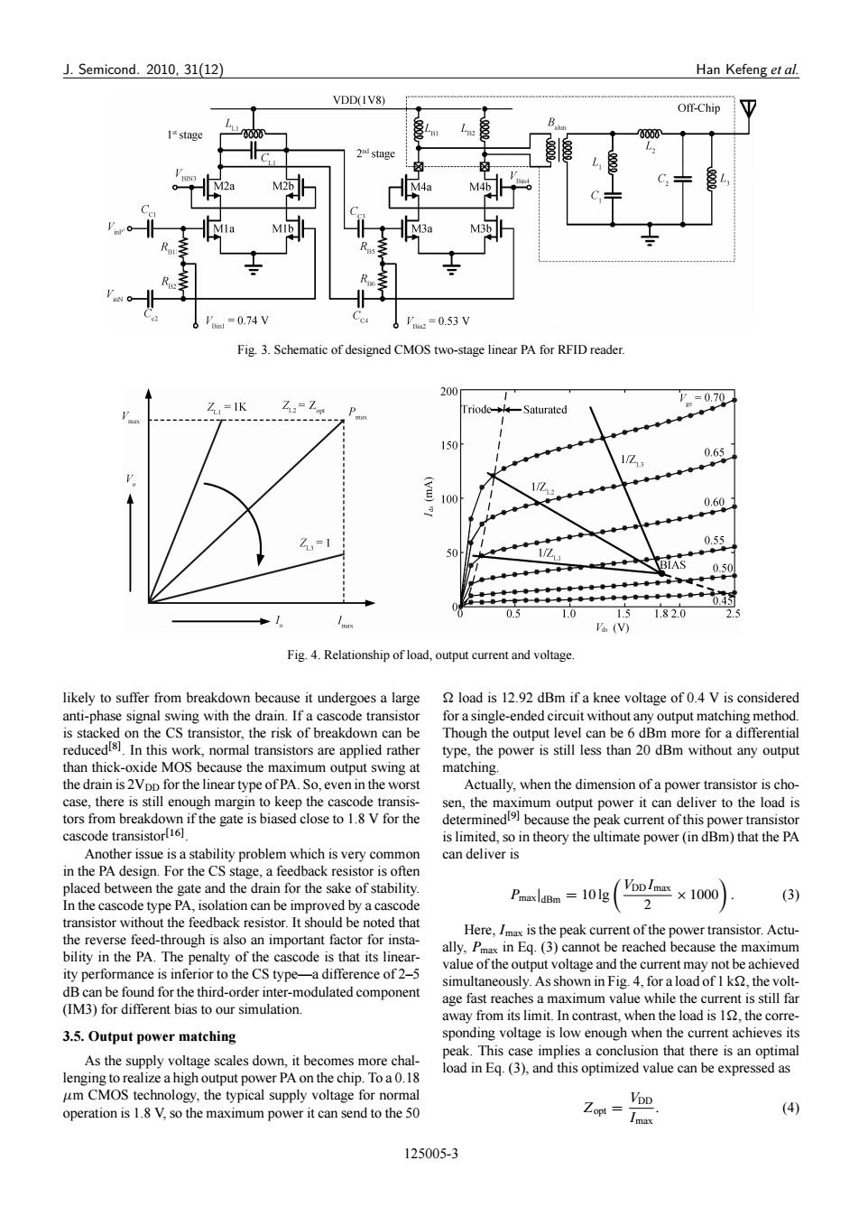
J.Semicond.2010,31(12) Han Kefeng et al. VDD(IV8) Off-Chip 1*stage 0000 2 stage M3 'a=0.74V a=0.53V Fig.3.Schematic of designed CMOS two-stage linear PA for RFID reader. 200 =0.70 Z=IK Z=Zon 150 0.65 Z 1/Z 2 0.60 Z=1 0.55 50 BIAS 0.5 1.5 1.82.0 (V) Fig.4.Relationship of load,output current and voltage likely to suffer from breakdown because it undergoes a large load is 12.92 dBm if a knee voltage of 0.4 V is considered anti-phase signal swing with the drain.If a cascode transistor for a single-ended circuit without any output matching method. is stacked on the CS transistor,the risk of breakdown can be Though the output level can be 6 dBm more for a differential reducedl).In this work,normal transistors are applied rather type,the power is still less than 20 dBm without any output than thick-oxide MOS because the maximum output swing at matching. the drain is 2Vpp for the linear type of PA.So,even in the worst Actually,when the dimension of a power transistor is cho- case,there is still enough margin to keep the cascode transis- sen,the maximum output power it can deliver to the load is tors from breakdown if the gate is biased close to 1.8 V for the determinedl]because the peak current of this power transistor cascode transistor[16]. is limited,so in theory the ultimate power(in dBm)that the PA Another issue is a stability problem which is very common can deliver is in the PA design.For the CS stage,a feedback resistor is often placed between the gate and the drain for the sake of stability PmaxldBm =101g VpDImax×1000 2 (3) In the cascode type PA,isolation can be improved by a cascode transistor without the feedback resistor.It should be noted that Here,Imax is the peak current of the power transistor.Actu- the reverse feed-through is also an important factor for insta- bility in the PA.The penalty of the cascode is that its linear- ally,Pmax in Eq.(3)cannot be reached because the maximum value of the output voltage and the current may not be achieved ity performance is inferior to the CS type-a difference of 2-5 dB can be found for the third-order inter-modulated component simultaneously.As shown in Fig.4,for a load of I k,the volt- age fast reaches a maximum value while the current is still far (IM3)for different bias to our simulation. away from its limit.In contrast,when the load is 19,the corre- 3.5.Output power matching sponding voltage is low enough when the current achieves its As the supply voltage scales down,it becomes more chal- peak.This case implies a conclusion that there is an optimal load in Eg.(3),and this optimized value can be expressed as lenging to realize a high output power PA on the chip.To a0.18 um CMOS technology,the typical supply voltage for normal VDD operation is 1.8 V,so the maximum power it can send to the 50 Zopt= Imax (4) 125005-3J. Semicond. 2010, 31(12) Han Kefeng et al. Fig. 3. Schematic of designed CMOS two-stage linear PA for RFID reader. Fig. 4. Relationship of load, output current and voltage. likely to suffer from breakdown because it undergoes a large anti-phase signal swing with the drain. If a cascode transistor is stacked on the CS transistor, the risk of breakdown can be reducedŒ8. In this work, normal transistors are applied rather than thick-oxide MOS because the maximum output swing at the drain is 2VDD for the linear type of PA. So, even in the worst case, there is still enough margin to keep the cascode transistors from breakdown if the gate is biased close to 1.8 V for the cascode transistorŒ16 . Another issue is a stability problem which is very common in the PA design. For the CS stage, a feedback resistor is often placed between the gate and the drain for the sake of stability. In the cascode type PA, isolation can be improved by a cascode transistor without the feedback resistor. It should be noted that the reverse feed-through is also an important factor for instability in the PA. The penalty of the cascode is that its linearity performance is inferior to the CS type—a difference of 2–5 dB can be found for the third-order inter-modulated component (IM3) for different bias to our simulation. 3.5. Output power matching As the supply voltage scales down, it becomes more challenging to realize a high output power PA on the chip. To a 0.18 m CMOS technology, the typical supply voltage for normal operation is 1.8 V, so the maximum power it can send to the 50 load is 12.92 dBm if a knee voltage of 0.4 V is considered for a single-ended circuit without any output matching method. Though the output level can be 6 dBm more for a differential type, the power is still less than 20 dBm without any output matching. Actually, when the dimension of a power transistor is chosen, the maximum output power it can deliver to the load is determinedŒ9 because the peak current of this power transistor is limited, so in theory the ultimate power (in dBm) that the PA can deliver is PmaxjdBm D 10 lg VDDImax 2 1000 : (3) Here, Imax is the peak current of the power transistor. Actually, Pmax in Eq. (3) cannot be reached because the maximum value of the output voltage and the current may not be achieved simultaneously. As shown in Fig. 4, for a load of 1 k, the voltage fast reaches a maximum value while the current is still far away from its limit. In contrast, when the load is 1, the corresponding voltage is low enough when the current achieves its peak. This case implies a conclusion that there is an optimal load in Eq. (3), and this optimized value can be expressed as Zopt D VDD Imax : (4) 125005-3�