正在加载图片...
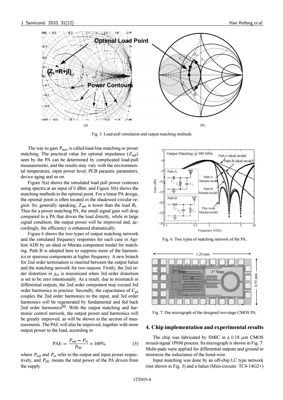
J.Semicond.2010,31(12) Han Kefeng et al. 055 下子2附 Optimal Load Point Z=R+i Power Contour吨 (a) (b) Fig.5.Load-pull simulation and output matching methods The way to gain Px is called load-line matching or power matching.The practical value for optimal impedance (Zopt) Output Matching 900 MHz Path-A ideal model seen by the PA can be determined by complicated load-pull Path-B ideal model measurements,and the results may vary with the environmen- tal temperature,input power level,PCB parasitic parameters, Path-A: 7 device aging and so on. Path-A Figure 5(a)shows the simulated load pull power contours -10 Murata mode using spectra at an input of 0 dBm,and Figure 5(b)shows the Path-B matching methods to the optimal point.For a linear PA design, Murata mode the optimal point is often located in the shadowed circular re- Path-B: gion.So,generally speaking,Zopt is lower than the load RL. This work Thus for a power matching PA,the small signal gain will drop Murata model compared to a PA that drives the load directly,while in large signal condition,the output power will be improved and,ac- 3 cordingly,the efficiency is enhanced dramatically. 0.1 0.5 Frequency (GHz) Figure 6 shows the two types of output matching network and the simulated frequency responses for each case in Agi- Fig.6.Two types of matching network of the PA. lent ADS by an ideal or Murata component model for match- ing.Path B is adopted here to suppress more of the harmon- 1.20mm ics or spurious components at higher frequency.A new branch for 2nd order termination is inserted between the output balun and the matching network for two reasons.Firstly,the 2nd or- der distortion in gm is maximized when 3rd order distortion dStage is set to be zero intentionally.As a result,due to mismatch in differential outputs,the 2nd order component may exceed 3rd order harmonics in practice.Secondly,the capacitance of Cgd couples the 2nd order harmonics to the input,and 3rd order harmonics will be regenerated by fundamental and fed back 2nd order harmonicsl6).With the output matching and har- monic control network,the output power and harmonics will Fig.7.Die micrograph of the designed two-stage CMOS PA. be greatly improved,as will be shown in the section of mea- surements.The PAE will also be improved,together with more output power to the load,according to 4.Chip implementation and experimental results The chip was fabricated by SMIC in a 0.18 um CMOS PAE=Pou-Pin x 100%. PDc (5) mixed-signal 1P6M process.Its micrograph is shown in Fig.7. Multi-pads were applied for differential outputs and ground to where Pout and Pin refer to the output and input power respec- minimize the inductance of the bond-wire. tively,and Ppc means the total power of the PA driven from Input matching was done by an off-chip LC type network the supply. (not shown in Fig.3)and a balun(Mini-circuits:TC4-14G2+) 125005-4J. Semicond. 2010, 31(12) Han Kefeng et al. Fig. 5. Load-pull simulation and output matching methods. The way to gain Pmax is called load-line matching or power matching. The practical value for optimal impedance (Zopt/ seen by the PA can be determined by complicated load-pull measurements, and the results may vary with the environmental temperature, input power level, PCB parasitic parameters, device aging and so on. Figure 5(a) shows the simulated load pull power contours using spectra at an input of 0 dBm, and Figure 5(b) shows the matching methods to the optimal point. For a linear PA design, the optimal point is often located in the shadowed circular region. So, generally speaking, Zopt is lower than the load RL. Thus for a power matching PA, the small signal gain will drop compared to a PA that drives the load directly, while in large signal condition, the output power will be improved and, accordingly, the efficiency is enhanced dramatically. Figure 6 shows the two types of output matching network and the simulated frequency responses for each case in Agilent ADS by an ideal or Murata component model for matching. Path B is adopted here to suppress more of the harmonics or spurious components at higher frequency. A new branch for 2nd order termination is inserted between the output balun and the matching network for two reasons. Firstly, the 2nd order distortion in gm is maximized when 3rd order distortion is set to be zero intentionally. As a result, due to mismatch in differential outputs, the 2nd order component may exceed 3rd order harmonics in practice. Secondly, the capacitance of Cgd couples the 2nd order harmonics to the input, and 3rd order harmonics will be regenerated by fundamental and fed back 2nd order harmonicsŒ6. With the output matching and harmonic control network, the output power and harmonics will be greatly improved, as will be shown in the section of measurements. The PAE will also be improved, together with more output power to the load, according to PAE D Pout Pin PDC 100%; (5) where Pout and Pin refer to the output and input power respectively, and PDC means the total power of the PA driven from the supply. Fig. 6. Two types of matching network of the PA. Fig. 7. Die micrograph of the designed two-stage CMOS PA. 4. Chip implementation and experimental results The chip was fabricated by SMIC in a 0.18 m CMOS mixed-signal 1P6M process. Its micrograph is shown in Fig. 7. Multi-pads were applied for differential outputs and ground to minimize the inductance of the bond-wire. Input matching was done by an off-chip LC type network (not shown in Fig. 3) and a balun (Mini-circuits: TC4-14G2+) 125005-4�