正在加载图片...
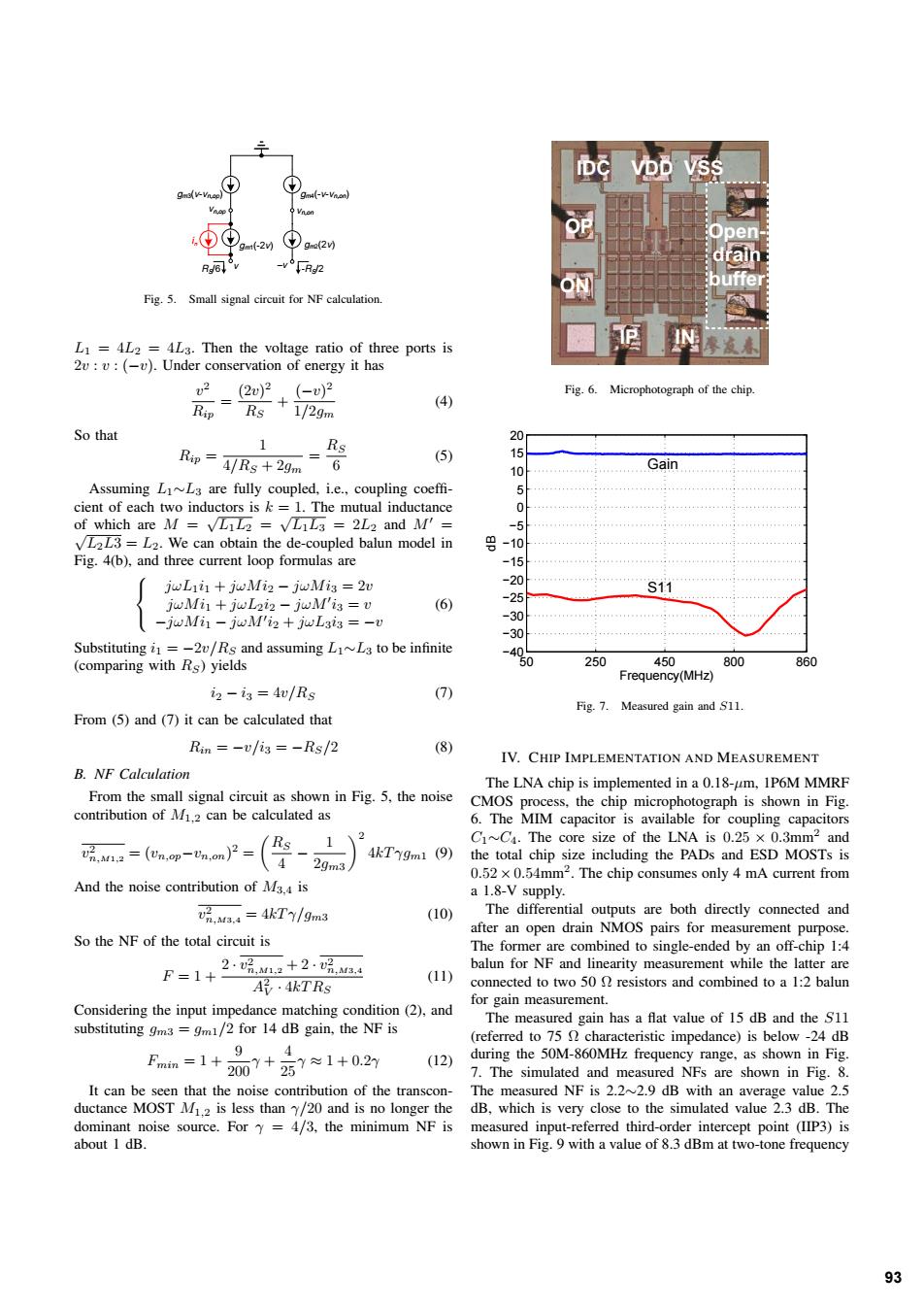
IDC VDD VSS gmsv-Vnep m(-V-Vna gm(-2v) ge(2) Rd6 v Fig.5.Small signal circuit for NF calculation. LI=4L2 =4L3.Then the voltage ratio of three ports is 2v:v:(-v).Under conservation of energy it has -2u2+-2 Fig.6.Microphotograph of the chip. Rip Rs129m (4) So that 20 1 Rs Rip=4/Rs +2gm 6 (5) 10 Gain Assuming L~L3 are fully coupled,ie.,coupling coeffi- 5 cient of each two inductors is k 1.The mutual inductance 0 小…小…小小…小小小小 of which are M VL1L2 VL1L3 2L2 and M'= -5 VL2L3=L2.We can obtain the de-coupled balun model in g-10 Fig.4(b),and three current loop formulas are -15 jwLiin jwMi2-jwMis=2v -20 S11 jwMin jwLi2-jwM'is =v (6) -25 -jwMin-jwM'i2+jwL3i3=-v -30 -30 Substituting i1 =-2v/Rs and assuming LI~L3 to be infinite -4 (comparing with Rs)yields 50 250 450 800 860 Frequency(MHz) i2 -i3=4v/Rs (7) Fig.7.Measured gain and S11 From (5)and (7)it can be calculated that Rin =-v/i3=-Rs/2 (8) IV.CHIP IMPLEMENTATION AND MEASUREMENT B.NF Calculation The LNA chip is implemented in a 0.18-um,1P6M MMRF From the small signal circuit as shown in Fig.5,the noise CMOS process,the chip microphotograph is shown in Fig. contribution of M.2 can be calculated as 6.The MIM capacitor is available for coupling capacitors (Rs 1 2 C~C.The core size of the LNA is 0.25 x 0.3mm2 and 2M1,2=(n,op-n,om)2= 4-2gm3 4kTygm1 (9)the total chip size including the PADs and ESD MOSTs is 0.52 x 0.54mm2.The chip consumes only 4 mA current from And the noise contribution of M3.4 is a 1.8-V supply. 2.wa4=4kT/9m3 (10) The differential outputs are both directly connected and after an open drain NMOS pairs for measurement purpose. So the NF of the total circuit is The former are combined to single-ended by an off-chip 1:4 F=1+ 2·哈M1,2+2·v2Md balun for NF and linearity measurement while the latter are (11) A·4kTRs connected to two 50 n resistors and combined to a 1:2 balun Considering the input impedance matching condition (2),and for gain measurement. substituting 9m3 =gm1/2 for 14 dB gain,the NF is The measured gain has a flat value of 15 dB and the S11 (referred to 75 characteristic impedance)is below-24 dB 9 4 Fmn=1+200Y+25Y≈1+0.2n (12) during the 50M-860MHz frequency range,as shown in Fig. 7.The simulated and measured NFs are shown in Fig.8. It can be seen that the noise contribution of the transcon- The measured NF is 2.2~2.9 dB with an average value 2.5 ductance MOST M12 is less than /20 and is no longer the dB,which is very close to the simulated value 2.3 dB.The dominant noise source.Fory=4/3.the minimum NF is measured input-referred third-order intercept point (IIP3)is about 1 dB. shown in Fig.9 with a value of 8.3 dBm at two-tone frequency 93v v ni gm3(v-vn,op) gm4(-v-vn,on) gm1(-2v) gm2(2v) vn,op vn,on RS/6 -RS/2 Fig. 5. Small signal circuit for NF calculation. L1 = 4L2 = 4L3. Then the voltage ratio of three ports is 2v : v : (−v). Under conservation of energy it has v2 Rip = (2v)2 RS + (−v)2 1/2gm (4) So that Rip = 1 4/RS + 2gm = RS 6 (5) Assuming L1∼L3 are fully coupled, i.e., coupling coeffi- cient of each two inductors is k = 1. The mutual inductance of which are M = √L1L2 = √L1L3 = 2L2 and M = √L2L3 = L2. We can obtain the de-coupled balun model in Fig. 4(b), and three current loop formulas are ⎧ ⎨ ⎩ jωL1i1 + jωMi2 − jωMi3 = 2v jωMi1 + jωL2i2 − jωM i3 = v −jωMi1 − jωM i2 + jωL3i3 = −v (6) Substituting i1 = −2v/RS and assuming L1∼L3 to be infinite (comparing with RS) yields i2 − i3 = 4v/RS (7) From (5) and (7) it can be calculated that Rin = −v/i3 = −RS/2 (8) B. NF Calculation From the small signal circuit as shown in Fig. 5, the noise contribution of M1,2 can be calculated as v2 n,M1,2 = (vn,op−vn,on) 2 = RS 4 − 1 2gm3 2 4kT γgm1 (9) And the noise contribution of M3,4 is v2 n,M3,4 = 4kT γ/gm3 (10) So the NF of the total circuit is F =1+ 2 · v2 n,M1,2 + 2 · v2 n,M3,4 A2 V · 4kTRS (11) Considering the input impedance matching condition (2), and substituting gm3 = gm1/2 for 14 dB gain, the NF is Fmin =1+ 9 200γ + 4 25γ ≈ 1+0.2γ (12) It can be seen that the noise contribution of the transconductance MOST M1,2 is less than γ/20 and is no longer the dominant noise source. For γ = 4/3, the minimum NF is about 1 dB. IP IN OP ON IDC VDD VSS Opendrain buffer Fig. 6. Microphotograph of the chip. 50 250 450 800 860 −40 −30 −30 −25 −20 −15 −10 −5 0 5 10 15 20 Frequency(MHz) dB Gain S11 Fig. 7. Measured gain and S11. IV. CHIP IMPLEMENTATION AND MEASUREMENT The LNA chip is implemented in a 0.18-μm, 1P6M MMRF CMOS process, the chip microphotograph is shown in Fig. 6. The MIM capacitor is available for coupling capacitors C1∼C4. The core size of the LNA is 0.25 × 0.3mm2 and the total chip size including the PADs and ESD MOSTs is 0.52 × 0.54mm2. The chip consumes only 4 mA current from a 1.8-V supply. The differential outputs are both directly connected and after an open drain NMOS pairs for measurement purpose. The former are combined to single-ended by an off-chip 1:4 balun for NF and linearity measurement while the latter are connected to two 50 Ω resistors and combined to a 1:2 balun for gain measurement. The measured gain has a flat value of 15 dB and the S11 (referred to 75 Ω characteristic impedance) is below -24 dB during the 50M-860MHz frequency range, as shown in Fig. 7. The simulated and measured NFs are shown in Fig. 8. The measured NF is 2.2∼2.9 dB with an average value 2.5 dB, which is very close to the simulated value 2.3 dB. The measured input-referred third-order intercept point (IIP3) is shown in Fig. 9 with a value of 8.3 dBm at two-tone frequency 93���